Introduction
The development in the field of bio sensing of biochemical molecules has been rapid during the recent years. Among many sensing technologies, Silicon Nanowire (SiNW)-based Field-Effect Transistors (FETs) have been shown to be as one of the most promising building blocks for the next generation electrical circuits in recognizing a wide range of biological and chemical targets. They have been successfully used in the detection of, for example, DNA, pH, protein, glucose, virus, and vapor. Despite the significant developments in the area, it seems, however, that the underlying detection mechanism and dynamics of the SiNW FETs are not well defined, and further studies are required. Due to the large surfaceto- volume ratio, one-dimensional nanostructures are considered as one of the best candidates for ultra-sensitive sensors. SiNW FETs have been experimentally demonstrated for direct, label-free, high sensitive, highly selective, and real-time detection of biological and chemical targets at very low concentrations. The most typical configuration of this device uses a nanowire as the essential building block bonding two ends of the nanowire to a solid substrate to create a SiNW FET.
Nanowire (NW) has attracted wide attention, and analyses that focus on various aspects of the device operation have accumulated. We have offered an experimental and analytical method to observe the poly silicon NW MOSFET threshold voltage based on a simple ballistic MOSFET modeling. This paper is intended to incorporate scattering effects into the ballistic modeling and to provide a compact model of the quasi-ballistic Si NW MOSFET. Silicon NW MOSFETs attract wide attention as a promising Nano device for future highdensity LSI application. For development of the device including the circuit application, a handy tool that affords accurate prediction of device characteristics is indispensable.
Device Design
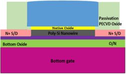
The device samples were manufactured on standard 6-in. p-type wafers. A proposed hybrid sensor/memory/CMOS poly-Si nanowire structure is illustrated in (Figure 1). The bottom-gate poly-Si nanowire formation can be inserted specifically after metallization of the back-end process (BEOL). At the beginning, buried oxide was deposited on a substrate surface as the gate dielectric of nanowire FETs. A 50-nm polysilicon layer was then deposited using the CVD process. Subsequently, the poly-Si wire was patterned by the standard I-line stepper of the CMOS semiconducting process. By using reactive plasma etching for photoresist trimming followed by silicon etching, the NW dimension was scaled to a level of approximately 100nm.

Figure 1: Cross-section of polysilicon nanowire.
A NW shrinkage technique using poly re-oxidation and oxide stripping was employed to scale down the NW width to less than 50nm. A channel protection photoresist pattern was then formed by I-line lithography. The objective of the channel protection patterning was to keep the channel intrinsically from n+ Source/Drain (S/D) heavy doping implantation, to increase NW FETs sensitivity.
Subsequently, the n+ S/D implant was performed with an ion beam to reduce the parasitic resistance of the NW. Thereafter, the channel protection photoresist was removed. Finally, the S/D dopant was activated by annealing treatment at higher temperature in a N2 ambience.
DNA Measurements, Data and Sensitivity Comparison
SiNW FETs have been shown to be as one of the most promising building blocks for the next generation electronic sensors in recognizing a wide range of biological and chemical targets such as DNA, pH, protein, glucose, virus, and vapor. At present, most SiNW FET detectors are fabricated with SOI wafer, in which the back-gate contact is used to control the conductivity of face oxide of the transistor. The SiNW with the box layer and the molecule (detection target) varies the surface potential of the surface oxide of the transistor.
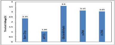
A compact model of I-V characteristics for a blastic NW MOSFET is proposed, and the device property is discussed. A new method to find the sensitivity of NW is proposed depending upon the drain saturation current (Ids). The electric current level in the saturation region shows the shift to show the sensitivity of the NW MOSFETs. It was experimentally found that the saturation current shows the sensitivity of the NW MOSFETs if the conventional method fails to show the sensitivity depending upon the Vth of NW MOSFET. As some NW MOSFETs have negative Vth therefore it’s difficult to see the sensitivity based upon Vth (Figure 2). So we propose that the sensitivity can be seen through the Ids and the Vth can also be determined by this method and our handy calculations. Also the native gate oxide on the undoped polysilicon increases the device reusability. The native oxide grows naturally on the polysilicon surface around 20-50 A which is the beauty of the device which increases the number of use in clinical process in day to day life.

    Figure 2:  Threshold sensitivity (a) threshold shift from bare chip to APTES
-55%, threshold shift from APTES to Glutaraldehyde 243%, and threshold
shift from Glutaraldehyde to ssDNA 13%, threshold shifts from ssDNA to
complementally dsDNA 3%.
Conclusion
Comparison of the silicon nanowire measurements on ssDNA and complementally dsDNA for both Vth and Ids saturation drain current has been performed, Comparison of the silicon nanowire measurements on SSDNA and dsDNA for both Vth and Ids saturation drain current has been performed, the results show that the Ids saturation drain current measurements has high sensitivity 55% from Glutaraldehyde to ssDNA and 44% from ssDNA to dsDNA. While for the Vth measurements, the sensitivity from Glutaraldehyde to ssDNA is 13% and 3% sensitivity from ssDNA to dsDNA. The use of Ids drain current measurement can also be easily implemented by simple electronic instrument since the current measurement is not sensitive by the gate voltage. The study will be continued to investigate for other types of DNAs.
