
Research Article
Austin J Nanomed Nanotechnol. 2014;2(2): 1014.
NSTOA-13-RA-108 Comparison of the Effects of Varying of Metal Electrode in Metal-Insulator-Metal Diodes with multi-dielectric layers
M. Alhazmi F1, Aydinoglu B. Cui1, O. M. Ramahi2, M. Irannejad1,2, A.Brzezinski1 and M. Yavuz1,*
1Waterloo Institute for Nanotechnology (WIN), University of Waterloo, Canada
2Electrical and Computer Engineering, University of Waterloo,Canada
*Corresponding author: M. Yavuz, Department of Mechanical and Mechatronics Engineering and Waterloo Institute for Nanotechnology University of Waterloo, Canada
Received: December 04, 2013; Accepted: January 24, 2014; Published: January 28, 2014
Abstract
Different metal–insulator–metal diodes using the fixedbottom electrode with different top electrodesandmulti–insulator layers were investigated. Chromium was usedfor the bottom metal electrode andTi, Cr, Al, and Pt were used asthe top metal electrode. The effects of tunneling junction and its effects in the diode performance were also studied. The high asymmetry value of 40, 16 and 6 were obtainedon applied voltage in the range of 0.5–3V respectively on using the Ti, Cr and Pt as the second metal electrode in the Metal–4 insulator layers–Metal diodes, while a combination of Cr–insulator layers–Al was shown relatively weak asymmetry curve.
Introduction
The demand for using a sufficient and clean source of energy is continuously increased. Therefore, investigation of a fast response time rectifying element is essential to overcome the issue of having insufficient rectification [1]. The best candidate rectifying diode is metal–insulator–metal (MIM) diode due to its advantages over semiconductor solar cells in terms of response time [2]. MIM diode is defined as a junction consisting of thin insulating layer (i.e. less than 10nm) between two metal electrodes [3,4]. Eventhough the architecture of this type of diode is simple; finding most suitable materials for producing high electrical performance is still a challenge. In addition to the insulator materials, there are some other important parameters such as current–voltage (I–V), nonlinearity, and asymmetry curves which affect the diode's performance. It is impossible to achieve both high asymmetry and nonlinearity by using MIM diodes with single insulator layer [5], and it has been reported that metal–double insulator–metal (MIIM) diodes can overcome this concern5. The insulator physical and chemical material properties such as work function [1],φ, electron affinity, χ, junction area, thickness and number of layers and their orders are the most important parameters that determine the MIM diode performance. The I–V curve strongly depends on the barrier height between the insulator and electrode and order of insulator. The potential barrier between the base electrode and the first insulator determines the turn on voltage, however, the potential barrier between the last insulator and top electrode determines the breakdown voltage according to the side of applied voltage.
Recently, P. Maraghechi et.al [6] studied the MIM diode structure with three insulator layers of Cr2O3–HfO2–Al2O3with different order. It was reported that the Cr/Cr2O3–HfO2–Al2O3/Cr diode exhibited a cascaded potential barrier profile; however non–cascaded profile wereobserved for the case of Cr/Cr2O3–Al2O3–HfO2/Cr diode. The former diode exhibited large degrees of asymmetry of (104) and nonlinearity (x=6).
Here, four different MIM diodes with multi–layers of insulators (i.e. four dielectric layers) by changing the top metal electrodes and keeping the bottom one fixed were studied. The I–V characteristics curve and asymmetrical, non–linearity curves of the fabricated diodes with different top electrode of Ti, Cr, Al, and Pt were also investigated.
Experimentand methodology
It is known that the insulator thickness changes the electron tunneling efficiency [1]. The tunneling process in the insulator layer is occurred at thickness of <10 nm. However, insulator thickness less than 4 nm is essential for achieving efficient tunneling. Therefore,in this study we were kept the total thickness insulator layers of all fabricated MIM devices as 3 nm to achieving high probability of the tunneling. A series of MIM diodes were fabricated on the SiO2 substrate to avoidthe conductivity of the substrate during the electrical characterization. In MIM fabrication, the first metal (bottom) electrode and insulator layers were fixed while different metals were used as the second metal (top) electrode as listed in table 1.
![]()
    MIM#
    Structure
    Work function(ev)


    1
    Cr-TiO2-Al2O3-TiO2-Al2O3-Ti
    -0.17


    2
    Cr-TiO2-Al2O3-TiO2-Al2O3-Cr
    >0


    3
    Cr-TiO2-Al2O3-TiO2-Al2O3-Al
    -0.22


    4
    Cr-TiO2-Al2O3-TiO2-Al2O3-Pt
    1.15
Table 1: MIM diode structureand their difference in work function that are used in this study.
Conventional photolithography followed by electron beam evaporation and atomic layer deposition (ALD) techniques, suitable technique for uniform, pinhole free and ultra–thin oxide film deposition due to its preciseness and controllability, were used for the fabrication of the MIM diodes on the SiO2 substrate. The insulator deposition process was carried by growing of one atom layer by one atom layer as discussed in the supplementary section. The SiO2 substrate was cleaned by acetone and isopropanol alcohol (IPA) and dried using nitrogen flow before each MIM fabrication. A layer of negative photo resist film (AznLOF 2035) up to thickness of 2.5 μm was coated onto the SiO2 substrate followed by soft–bake at 1100 © for one minute to drive off solvent and increasing the adhesion between the photo resist film and sample. The photo resist film was patterned using contact mask aligner (Karl Suss MA6). After proper exposure time, the sample was baked at 1100C to speed up the cross–linking of the photoresist and developed in AZ300MIF for one minute and rinsed by IPA followed by DI water for one minute and dried underN2flow.
Electron–beam evaporation technique was used to deposit 60nm of chromium as bottom electrode. ALD technique was utilized to deposit TiO2 (I1) and Al2O3(I2)at rates of 0.044±0.001 nm/cycle and 0.105±0.001 nm/cycle, respectively (supplementary part). The insulators deposition was repeated for 2cyclesin order to obtain a total number of insulators of four. Each insulator was 0.75nm thick, giving a total barrier thickness of 3nm. Photolithography process was carried out in order to align the structure and finishing the whole device fabrication. In last step electron beam evaporation was utilized to deposit the second metal (top) electrode of 100 nm thick. Fig.1 shows the schematic diagram the MIIIIM diode structure and SEM micrograph of the MIIIM diodes of different overlapping area of 10 μm, 20 μm and 30 μm is shown in Figure 2.
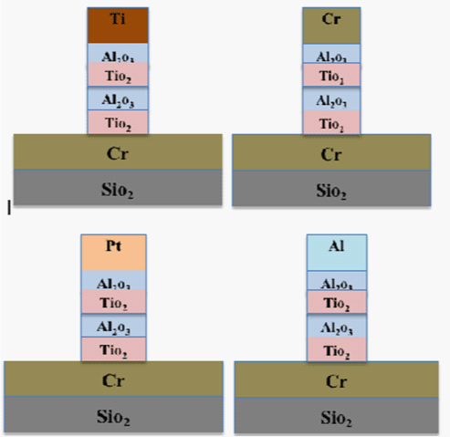
Figure 1: A schematic diagram of the cross-sectional view of the Cr-TiO2-Al2O3-TiO2-Al2O3-Ti, Cr-TiO2-Al2O3-TiO2-Al2O3-Cr, Cr-TiO2-Al2O3-TiO2-Al2O3-Al and Cr-TiO2-Al2O3-TiO2-Al2O3-Pt diodes.
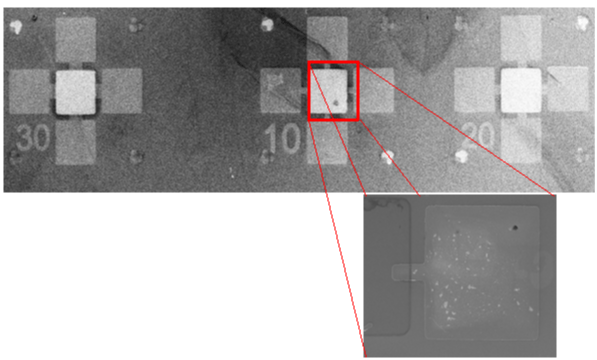
Figure 2: SEM image of the Cr-TiO2-Al2O3-TiO2- Al2O3-Ti diode structure at different size of the overlapping area of a) 10 μm, b) 30 μm, c) 30 μm.
Results and Discussion
The two and four insulator layers Cr–Insulator– M diodes were studied by comparing the I–V, asymmetry and nonlinearity curves. In this structure the M stands for Ti, Al, Pt and Cr. The I–V measurement was carried out using Keithley 4200–SCS semiconductor characterization system and the applied voltage was considered in the range of –6 V to 6 V. Asymmetry and nonlinearity of the fabricated diodes were calculated using following equations:
Here IF, IR, dI, dV and V are forward current, breakdown current, and applied voltage respectively.
In order to have optimal behavior of the MIM diodes, the insulator layer requires a low surface roughness, uniform thickness, and stoichiometry which can be achieved by having a small device area [7] (i.e. μm2 or less). Four combinations of quadra insulator MIM diodes with different work functions, Δ φ (= φ2 - φ1), as listed in table 1 were fabricated and characterized.The work function of the base electrode, Cr, was considered asφ1=4.5eV. In Fig.3the current–voltage response of fabricated structures with double insulator layers (red curve) and four insulator layers (blue curve) were compared. From this figure it is clear that the current resulted from diodes of four insulator layers was much larger than the case of two insulator layers. This could be attributed to the electron tunneling process via aid of a quantum well structure observed in the case of forwarded biased voltage. Whilst on using a reverse bias, there is no evidence of quantum well formation and thus electrons must tunnel through all barriers without any assistance which results in a highly nonlinear and asymmetric I–V curve. It is hard to achieve both high conductivity and nonlinearity due to tradeoff between conductivity and nonlinearity. Hence devices with two insulators exhibited more nonlinearity; however, conductivity showed better performancewhenfour insulator layers were used as shown in Figure 3. From this figure, it is also clear that the MIM diodes using, Craned Pt as top electrodes exhibited the most asymmetric properties. This could be attributed to their band gap energy offset at the interface which affects the tunneling current through insulating layers.
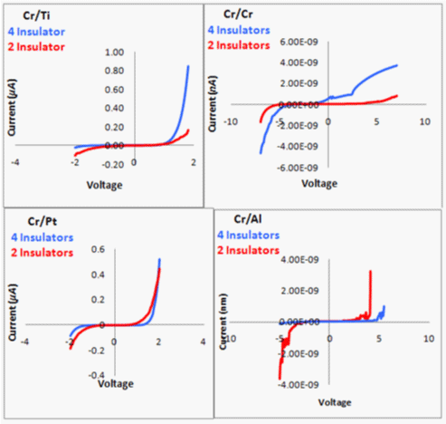
Figure 3: The I-V characteristics curve of the a) Cr-I1I2I1I2-Ti and Cr-I1I2-Ti , b) Cr- I1I2I1I2-Cr and Cr- I1I2-Cr, c) Cr- I1I2I1I2-Al and Cr-I1I2-Al,d) Cr-I1I2I1I2-Pt and Cr-I1I2-Pt diode.
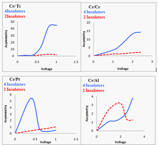
Figure 4: Asymmetry curve of the fabricated diodes: a) Cr-Al2O3-TiO2- Al2O3- TiO2-Ti, b) Cr-Al2O3-TiO2- Al2O3-TiO2-Cr, c) Cr-Al2O3-TiO2- Al2O3-TiO2-Al, d) Cr- Al2O3-TiO2- Al2O3-TiO2-Pt.
The barrier heights of device’s interface were calculated for difference fabricated diodes and were reported in table 2. The electron affinity of 0.75nm layer of the TiO2 and Al2O3 was reported as 4.3 eV, and 3.5 eV [8], respectively. Since each diode has five interfaces, the barrier heights are given by:
![]()
    MIM#
    Φ1 = φ1− χ1(ev)
    Φ2 = Φ3 = Φ4 = χ1 − χ2(ev)
    Φ5 = φ2 − χ2(ev)


    1
    0.2
    0.8
    0.83


    2
    0.2
    0.8
    1


    3
    0.2
    0.8
    0.78


    4
    0.2
    0.8
    2.15
Table 1: Barrier height potential of fabricated CrI1I2I1I2M diodes.
Φ1 = φ1− χ1 (3)
Φ2 = Φ3 = Φ4 = χ1 − χ2 (4)
Φ5 = φ2 − χ2 (5)
By applying voltage to M electrode (e.g.Ti), Ti electrons tunneled through aultra–thin oxides. As a result, an electrical current was created from base electrode (Cr) towards the M electrode.
Figure.4 compares the asymmetry curves of the MI1I2I1I2M and the diodes with the applied voltage in the range of 0.5–3V. As can be seen from this figure when the Ti was used as the top electrode in the MI1I2I1I2M structure (blue curve) the highest asymmetry value of40 was achieved at a voltage of 1V; while whenMI1I2M structure (red curve) was used the asymmetryof nearly equal to 1 was obtained. It was found that when Pt was used as the top electrode, the asymmetry was 6at an applied voltage value of 0.5V. And much smaller asymmetry of 1, was calculated in whenCrI1I2Pt structure was used. When Cr was used for both metal electrodes and four insulator layers, the I–V curve was highly asymmetric with a value of 16 at an applied voltage of 2V as seen in Figure.4b.However, this structure consists of the same metal electrodes (Cr), for that reason, there was still a work function difference between the two electrodes. The reason of such a low barrier height might be due to the difference among processing conditions of the electrodes [9]. The forward current, defined as the flux of electrons tunneled from top electrode to the base one (Cr), was larger than the reverse current, and due to this tunneling there would be an inherited work function difference. Since the asymmetry of the MIM diode is a function of the applied voltage, the amount of voltage bias affects the asymmetry values obtained in this research. Figure.4 also shows a low asymmetry when a combination of Cr and Al was used as base and top electrodes, respectively, especially for the MI1I2I1I2Mstructures at an applied voltage of 1V. Because of a bias voltage applied to the Al electrode, the A electrons tunneled through the thin barrier with a total thickness of 3nm. The amplitude of the current obtained using Cr electrode depends on the barrier heights as well as on the applied voltage. It can be concluded that the increase in asymmetry was not a linear function of the work function difference between base and top electrodes. This conclusion in fact is in a good agreement with the literature [10].
Conclusion
In this work, different MI1I2I1I4M diodes structures were fabricated and their performance was compared. The characterization of these various diodes was performed by measuring their I–V electrical responses. The MIIIIM diodes using Ti and Cr, and Pt as the second metal electrode exhibited a superior performance in terms of asymmetry; while a combination of Cr–insulator –Al showeda relatively lower asymmetry curve.
References
- Eliasson B J. metal-insulator-metal diodes for solar energy conversion .PhD thesis. University of Colorado. Boulder.2001.
- Da Costa V, Romeo M, Bardou F. Statistical properties of currents flowing through tunnel junctions. Journal of Magnetism and Magnetic Materials. 2003; 258: 90-95.
- Krishnan S, Stefanakos E, Bhansali S. Design and development of batch fabricatable metal-insulator-metal diode and microstrip slot antenna as rectenna elements. Thin Solid Films. 2008; 516: 2244-2250.
- Dagenais M, Choi K, Yesilkoy F, Chryssis A, Peckerar M. Solar spectrum rectification using nano-antennas and tunneling diodes. Optoelectronic Integrated Circuits XII,Proceedings of the SPIE. 2010; 7605: 76050-76050.
- Grover S, Moddel G, IEEE Journal of Photovoltaics. Applicability of Metal/Insulator/Metal (MIM) Diodes to Solar Rectennas. 2011; 1: 78-83.
- Maraghechi P, ForoughiAbari A, Cadien K, and Elezzabi AY. Observation of resonant tunneling phenomenon in metal-insulator-insulator-insulator-metal electron tunnel devices.Appl. Phys. Lett. 2012; 100: 113503.
- Tien TC1, Pan FM, Wang LP, Lee CH, Tung YL, Tsai SY, et al. Interfacial energy levels and related properties of atomic-layer-deposited Al2O3 films on nanoporous TiO2 electrodes of dye-sensitized solar cells. Nanotechnology. 2009; 30: 305201.
- Periasamy P, Berry J, Dameron A, Bergeson JD, Ginley DS, O'Hayre R. P, Parilla P. A. Fabrication and Characterization of MIM Diodes Based on Nb/Nb2O5 Via a Rapid Screening Technique.Adv. Mater. 2011; 23: 3080-3085.
- Hashem I. E, Rafat N. H, Soliman E. A. Theoretical Study of Metal-Insulator-Metal Tunneling Diode Figures of Merit. IEEE Journal of Quantum Electronics.2013; 49: 72-79.
- Choi K, Yesilkoy F, Ryu G, Cho S. H, Goldsman, N, Dagenais M,Peckerar M. A. Fabrication of Thin Film Asymmetric Tunneling Diode using Geometric Field. Enhancement. IEEE Trans. Electron Devices. 2011; 58: 3519-3528.