
Review Article
Austin J Chem Eng. 2014;1(1): 1002.
Structural and Optical Properties of Nanocrystalline Cuxs Solid Thin Films
Singh Ajaya Kumar1*, Mehra Swati2 and Thool Gautam Sheel1
1Department of Chemistry, Govt. VYT PG Autonomous College, Durg, 491001 (C.G.), India.
2Department of Chemistry, Rungta College of Engineering and Technology, Bhilai, 490024, (C.G.), India.
*Corresponding author: Singh Ajaya Kumar, Department of Chemistry, Govt. VYT PG Autonomous College, Durg, 491001 (C.G.), India
Received: April 28, 2014; Accepted: May 26, 2014; Published: May 27, 2014
Abstract
Copper sulphide thin films were deposited by chemical bath deposition method at 65oC. These were then annealed at 100°C and 200°C. All films exhibit nanocrystalline nature, having Chalcosite low phase, with grain size ranging from a minimum of 5.71nm to maximum of 30.67nm. Effect of annealing shows increased grain size nano-thin film formation. Optical properties show that films can find application in optoelectronic devices as band gap ranging between minimum of Eg = 2.64 eV to highest of 2.92 eV. AFM studies shows that nanothin film formed has spiky and bumpy surfaces.
Keywords: Copper sulphide; Chemical bath deposition; Thermal annealing; XRD; Optical properties
Introduction
It is found that CuxS thin films act as p-type semiconductor material mainly due to that of copper vacancies occurring within the lattice [1,2] and its variable property exhibition depending upon the stoichiometry, 1 ≥ x ≥ 2. Due to variable optical and electrical properties this found to have many potential applications in various fields as in solar cells, fluorescent devices [3-10], photo thermal conversion of solar energy, microwave shielding coatings, electro conductive electrodes, catalyst [11-14], selective radiation filters, photodetectors, as polarizers of infrared radiation [15], active absorbent of radio waves [16], semiconductors, electroconductive coatings, low temperature gas sensor applications [17], field emission [18], switching [19], sensing devices [20], themoreflecting coatings [21], eyeglass coatings, anti reflecting coatings [22], thermoelectric cooling materials [23], optical filters, optical recording materials, nanoscale switches, and superionic materials [24] etc. Copper sulphide at room temperature occurs in five stable phases namely: covellite (Cu1.00S), anilite (Cu1.75S), digenite (Cu1.80S), djurleite (Cu1.97S), and chalcocite (Cu2.00S). Other phases that exist include yarowite (Cu1.12S) and spionkopite (Cu1.14S).
It has been found that Cu2-xS exists in four crystallographic modifications. The monoclinic phase, low-chalcocite (αCh) is stable up to temperatures between 90 - 104°C, depending on the chemical composition x's. Above 90°C, the hexagonal phase, high-chalcocite (βCh) is stable. At a composition close to x = 0, this phase is stable up to 435°C. The third, cubic phase called digenite (Dg-Cu2-xS), stable between temperatures of 72 - 1130°C. The fourth crystallographic modification being orthorhombic phase denoted as djurleite (Dj), which is stable up to a temperature of 93°C. The compound Cu7S4 denoted as anilite (An) is stable up to 75°C. The copper sulfide, CuS (covellite, Cv), is stable up to a temperature of 507°C. Several phases of copper sulfides are metastable, but these may convert to the thermodynamically more stable ones. For example, after a few hours, the high digenite (Cu1.80S) began to convert into the low digenite (Cu1.765S), which in turn, converts to anilite (Cu1.75S) [25,26]. At 41°C, anilite decomposes into CuS and low digenite, whereas low digenite transforms into high digenite around 82°C [25,27].
For reproducing copper sulphide thin films, chemical bath deposition method is being opted, because it is a low cost simple method, a large area of deposition is available which can occur at a low temperatures. Principle of CBD method follows a controlled chemical reaction which eventually leads to deposition of thin film by precipitation. CBD method involves specified reaction conditions, which generally involves substrates immersed in a beaker having an alkaline solution containing chalcogenide source ions, metal ions and added base, where complexing agent is being added to control release of metal ion. This process itself depends on various parameters like ionic product, solubility product, super saturation, type of precipitation etc.
In the present paper, an attempt is made to deposit nano crystalline thin film of copper sulphide on glass substrates by chemical bath deposition method. Effect of variation in chemical bath composition on the structural and optical properties has been studied specifically for as-deposited and post deposited thermal annealed thin films.
Experimental Details
Preparation of Glass Substrate
For deposition of thin film, glass substrate (micro slides - 75mm L x 25 mm wide) were taken. Pretreatment of glass substrate follows:-
- Wash with normal water 2 - 3 times
- Soak them in chromic acid for 48 hrs. - 120 hrs.
- Boil them for one hour in chromic acid itself.
- Wash by deionised water several times.
- Washing them with detergent solution.
- Then Micro slides cleaned with tap water and further by deionised water.
- Degreased with ethanol, washed with deionised water in ultrasonicator and air dried.
- Eventually preheat the slides in the oven before use.
Preparation of CuS thin film
To prepare Copper sulphide thin films, 10 ml of 0.1 M CuSO4.5H2O (Cu2+ ion source) and 10 ml of 0.1 M C4H6O6 (being used as complexing agent) were taken in 50 ml beaker. After constantly stirring for 5 min, add 1 ml NH3 and 3ml or 4ml of TEA concentration, to obtain reaction pH maintained1.02 .9� . Other than for maintaining optimum pH for reaction bath, the concentration of TEA was varied over a wide range and optimized condition was found to be 3 ml and 4 ml for adherent and uniform thin film deposition. This followed by addition of 10 ml of 0.1 M (NH2)2CS ( S2- ion source). Stir the solution for 20 to 25 min. Keep the reaction mixture in a water bath at 65°C with vertically placed slides in it. After 180 mins, slides were taken out from reaction bath (the temperature and deposition time being controlled over for good deposition of thin film on glass substrate and optimum condition found for stable adherent film deposition). The slides which were taken out washed with deionised water and air dried. Out of two sets of slides (three slides each), one slides restored as-deposited slides, other two annealed at 100°C, 200°C for an hour in the oven. The slides, S1 and S4 being as-deposited / 180 min for 1:3 and 1:4 ratio of NH3: TEA, S2 and S5 are being their annealed samples at 100°C and S3 and S6 annealed sample at 200°C.
Mechanism of thin film formation
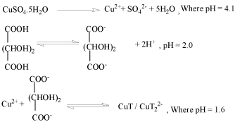
Figure 1 : The growth mechanism is proposed by the following reaction steps:
With addition of NH3 and TEA, pH of chemical bath was maintained at 1.02.9� .When the pH increases, there is an increasing tendency for the formation of mixed ligand complexes or hydroxyl complexes. With copper cations, this equilibrium can be expressed by the following equilibriums:-
Cu2++2 OH- +2 T2- ⇔ CuT2(OH)24-
Other than above complex, TEA and NH3 form complex with availability of free copper ions present in reaction bath, as both TEA and NH3 have tendency to act as complexing agent also. Thus helps in reduced growth phase of the thin film or controlling the concentration of free Cu2+ ions.
Cu2+ +4 (NH3) → [Cu(NH3)4]2+
Cu2+ +n (TEA) → [Cu(TEA)n]2+
Therefore tartaric acid, TEA and NH3 results in the coexistence of different copper complexes in the bath.
Eventually with addition of thiourea in the reaction mixture, can result in following reactions:-
(NH4)2CS +O H- → CH2N2 +H S- +H2O
HS- +O H- → S2- +H2O
This result in following cases of copper sulphide thin film formation:-
CuT + S2- → CuS + C4H4O62-
CuT22- + S2- → CuS + 2T2-
[CuT2(OH)2]4- + CS(NH2)2 → CuxS + 3H2O + OC(NH2)2 + By Products
[Cu(NH3)4]2++ CS(NH2)2 + 2OH- → CuS + NH3 + CN3H5 + H2O
[Cu(TEA)n]2++ CS(NH2)2 + OH- → Cu2S +(NC-NH2) + 2H2O
[Cu(TEA)n]2++ CS(NH2)2 + OH-+ H2O → CuS + OC(NH2)2 + nTEA+ 3H2O
Characterization of thin film
The X-ray diffraction (XRD) patterns were recorded to characterize the phase and structure of the thin films using a Bruker D8 advance X ray diffractometer with CuKα radiation (40 kV and 40 mA) with λ = 1.54 � for 2θ° values over 20°-80°. The surface morphology and topography of CuS thin film were examined using atomic force microscopy (AFM) having details as AFM model-NSE (Nano scope-E), AFM mode-Contact mode AFM, Tip Material-Si3N4 (Silicon Nitride). Optical absorption data were obtained with a Cary Bio 50 Varian UV-Vis spectrophotometer at normal incidence of light in the wavelength range of 200-1000 nm. Thickness measurements of thin film were done by surface profiler.
Results and Discussion
XRD Studies
The X-ray diffraction was carried out for six samples, respectively, as-deposited and annealed (at 100°C, 200°C) of thin films and their diffractograms being shown respectively in Figure I (a) and (b). Sample S1 shows orthorhombic Cu2S phase of copper sulphide, but shows very small peaks, but two peaks clearly identified. The peaks at angles 2θ°, reflection from crystal peaks from corresponding standard 2θ° as from JCPDS card being shown in Table I. From this it's been found that annealing effectively increases crystalline nature of thin films. Table II shows the average grain size calculated by:-
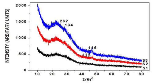

Figure 1 (a): XRD pattern of as-deposited, annealed (100°C, 200°C) copper sulphide thin films with 3 ml TEA, 180 min deposition time.
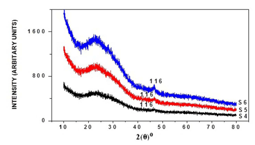
Figure 1(b): XRD pattern of as-deposited, annealed (100°C, 200°C) copper sulphide thin films with 4 ml TEA, 180 min deposition time.
![]()
    S.No.
    Sample
    Obs. 2θ°
    Std.2θ°
    hkl planes
    Phase and System


    1
    S 1
    28.333
      37.452
    28.309
      37.506
    421
      1 11 1
    Cu2S Orthorhombic


    2
    S 2
    46.111
    46.559
    116
    Cu2S Orthorhombic


    3
    S 3
    28.014
    28.026
    262
    Cu2S Orthorhombic


    32.375
    32.472
    134


    46.314
    46.559
    116


    4
    S 4
    46.341
    46.559
    116
    Cu2S Orthorhombic


    5
    S 5
    46.503
    46.559
    116
    Cu2S Orthorhombic


    6
    S 6
    46.588
    46.559
    116
    Cu2S Orthorhombic
Table 1: Comparison of observed XRD data of thin films with the JCPDS cards (Cu2S: 23-0961).
![]()
    I
    II
    III
    IV
    V
    VI
    VII


    Sample.
      No.
    Obs
      2-theta
    Standard
      2-theta
    d-spacing
    Grain Size
      D (nm)
    Dislocation    density (δ) x1014 Line's m-2
    Microstrain    (ε) x10-3


    S1
    -
    -
    -
    -
    -
    -


    S2
    46.111
    46.559
    1.95
    11.82
    7.16
    7.41


    S3
    28.014
    28.026
    1.96
    7.15
    19.58
    12.33


    S3
    32.375
    32.472
    3.18
    14.59
    4.7
    9.81


    S3
    46.314
    46.559
    5.53
    5.71
    30.67
    21.77


    S4
    46.341
    46.559
    1.96
    3.15
    7.1
    28.06


    S5
    46.503
    46.559
    1.95
    30.60
    1.07
    2.89


    S6
    46.588
    46.559
    1.95
    36.97
    7.3
    2.37
Table 2: Showing 2θ°, d-spacing, average crystallite size, dislocation and micro strain of sample S 1 - S 6 thin film.
Average Micro strain
Dislocation density (lines m-2) by Williamson Smallman's formula
D-Spacing by Bragg's equation
Optical Studies
From Figure II (a) and (b) absorbance decreases in order of S 2 > S 1 > S 3 and S 4 > S 5 > S 6 respectively, while % transmittance decreases in order of S 3 > S 2 > S 1 and S 6 > S 5 > S 4. The optical band gap has been found to be 2.92eV, 2.8eV, 2.64eV, 2.9eV, 2.94eV, 2.9eV as for S 1- S 6 samples individually as shown in Figure II (c) and (d), having thickness of film 150 nm, 20 nm, 15 nm, 200 nm, 70 nm, 20 nm in the order of samples for S 1, S 2, S 3, S 4, S 5, S 6 respectively. On the basis of absorbance variation the annealed samples can be effective in reducing solar reflectance side by side helps in increasing transmittance, and can prove to be an effective material for AR coatings. The decrease in value of band gap shows the transition of poor crystallinity towards polycrystalline nature that is annealed sample being more crystalline as compared to as-deposited samples.
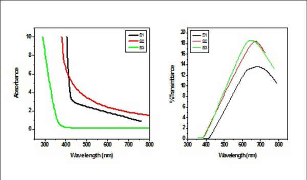
Figure2 (a): Absorbance and % transmittance of S 1-S 3 copper sulphide thin films.
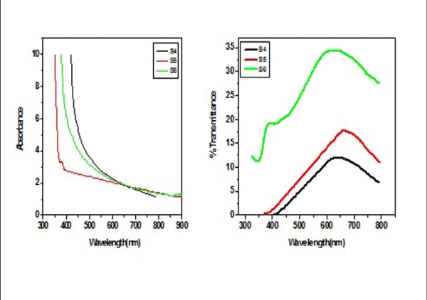
Figure 2(b): and % transmittance of S 4 -S 6 copper sulphide thin films.
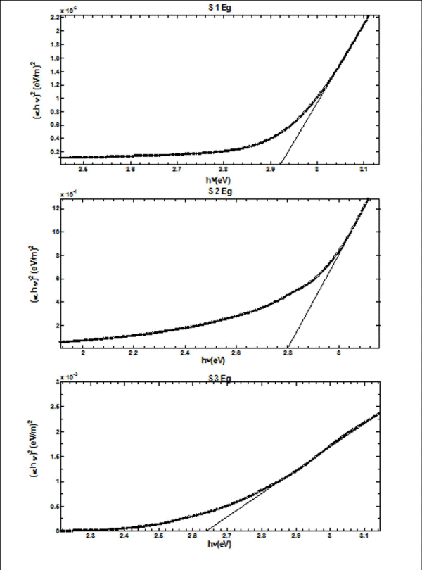
Figure 2(c): Optical Band Gap (Eg) for S 1 - S 3 copper sulphide thin films.
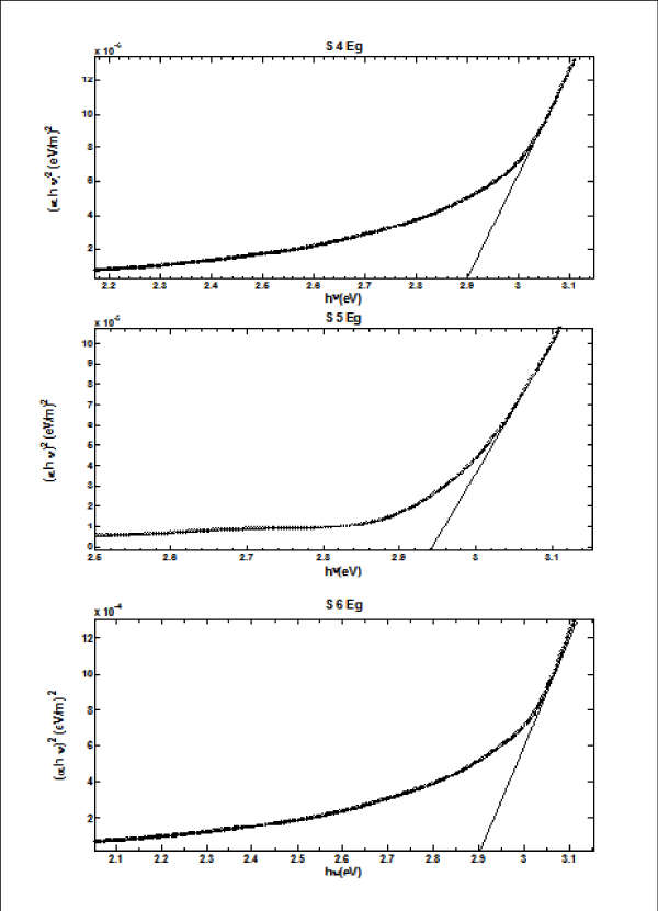
Figure 2 (d): Optical Band Gap (Eg) for S 4 - S 6 copper sulphide thin films.
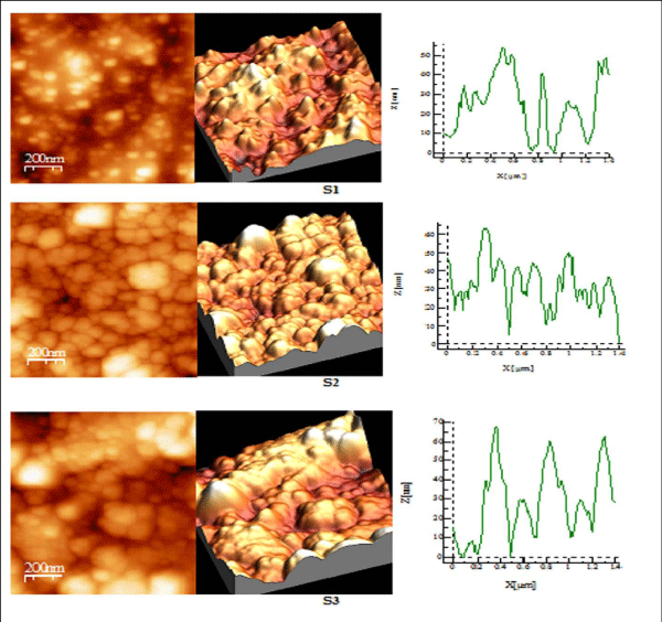
Figure 3 (a): AFM study of S 1-S 3 copper sulphide thin films.
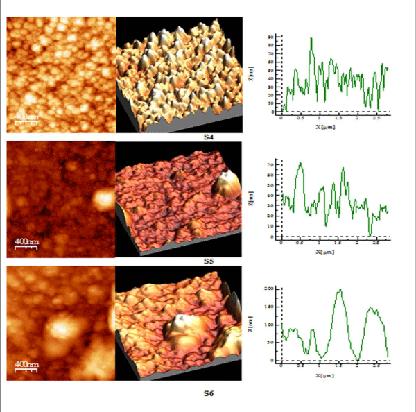
Figure 3 (b): AFM study of S 4-S 6 copper sulphide thin films.
AFM Studies
AFM studies reveal that annealed samples have greater surface quality as compared to their as-deposited samples as shown in Table III, RMS roughness of thin film increases on annealing showing that grain size increases after annealing process [28,29]. S1 and S2 have spiky surface as Rku> 3, while on greater annealed temperature film shows the bumpy surface as Rku< 3 i.e S3. The surface profile picture of S1, S2, S3, shows that size of particles is nanoparticles. S4 sample having good bearing surface as have negative skewness, while S5 sample has a large number of spikes all over the surface also been cleared by value of Rku being 16.82, as well from 3D picture also Rsk> 3 [30], while S6 has highest RMS roughness, has the best surface quality among all, having spiky surface Rku> 3.
![]()
    I
    II
    III
    VI
    V


      S. No.

      Sample

      RMS (root    mean square) Roughness

      Surface    Skewness (Rsk)

      Surface    Kurtosis (Rku)


    1
    S 1
    14.97
    0.59
    3.08


    2
    S 2
    18.72
    0.67
    3.69


    3
    S 3
    26.85
    0.37
    2.47


    4
    S 4
    18.84
    -0.005
    2.84


    5
    S 5
    28.60
    3.15
    16.82


    6
    S 6
    44.62
    0.86
    3.76
Table 3: Showing RMS roughness, surface skewness and surface kurtosis of sample S 1 - S 6.
Conclusion
It is seen that bath composition effectively help in increasing the band gap, and that annealing also help to improve the structural and optical properties of thin film. Here it also been observed that concentration ratio of NH,sub>3
: TEA effect deposition of thin film on substrate. Higher concentration of NH3 more than 1ml, and TEA concentration more than 4- 5 ml result in poor deposition of thin film on glass substrate.As compared to the as-deposited thin films, annealed samples showed increased crystallinity. The AFM study shows that on annealing, the surface roughness increases, which explain that coalescence of grain, occur after annealing at higher temperatures. The band gap decreases on annealing in some samples which shows that on annealing crystallinity of thin film increases.
Acknowledgement
We are grateful to UGC-DAE Consortium for Scientific Research INDORE-CENTRE, DAVV Campus, Khandwa Road, Indore 452017, and India. Authors are thankful to Prof. Ajay Gupta for providing the experimental facilities at UGC-DAE CSR Indore. Authors are also thankful to Dr. Mukul Gupta for XRD measurements, Dr. V. Ganesan and Mr. Mohan Gangarade extending the AFM measurements, Dr. D.M Phase and Mr. Manoj Kumar for thickness measurements.
References
- Li S, Wang H, Xu W, Si H, Tao X, Lou S, et al. Synthesis and assembly of monodisperse spherical Cu2S nanocrystals. J Colloid Interface Sci. 2009; 330: 483-487.
- Wu Y, Wadia C, Ma W, Sadtler B, Alivisatos AP. Synthesis and photovoltaic application of copper(I) sulfide nanocrystals. Nano Lett. 2008; 8: 2551-2555.
- Sartale SD, Lokhande CD. Growth of copper sulphide thin films by successive ionic layer adsorption and reaction (SILAR) method. Mater. Chem. Phys; 2000; 65: 63-67.
- Lindroos S, Arnold A, Leskela M. Growth of CuS thin films by the successive ionic layer adsorption and reaction method. Appl. Surf. Sci. 2002; 158: 75-80.
- Grozdanov I, Najdoski M. Optical and electrical properties of copper sulfide films of variable composition. J. Solid State Chem. 1995; 114: 469-475.
- Dhar S, Chakraborti S. Properties of chemically deposited Cu2S films on porous silicon. J Appl Phys.1997, 82: 655-657.
- Nickless G. Inorganic Chemistry of Sulfur. Elsevier. London. 1968; 670.
- Greenwood NN, Earnshaw EA. Chemistry of the Elements, Pergamon. Oxford. 1990; 1403.
- Partain LD, Schneider RA, Donaghey LF, Mcleod PS. Surface chemistry of Cu x S and Cu x S/CdS determined from x-ray photoelectron spectroscopy. J Appl Phys. 1985; 57: 5056-5065.
- Nair PK, Nair MTS. Chemically deposited SnS-CuxS thin ?lms with high solar absorptance: new approach to all-glass tubular solar collectors. J Phys D. 1991; 24: 83-87.
- Yamaguchi T, Yamamoto Y, Tanaka T, Demizu Y, Yoshida A. (Cd,Zn)S Thin Films Prepared by Chemical Bath Deposition for Photovoltaic Devices. Thin Solid Films. 1996; 281: 375-378.
- Teteris J. Holographic recording in amorphous chalcogenide thin films. Current Opinion in Solid State and Materials Science. 2003; 7: 127-134.
- Savadogo O. Chemically and Electrochemically Deposited Thin Films for Solar Energy Materials. Sol. Ener. Mat. Sol. Cells. 1998; 52: 361-388.
- Sang B, Shafarman WN, Birkmire RW. 29th IEEE Photovoltaics Specialists Conference. 2002.
- Nair MTS, Nair PK. SnS�CuxS thin-film combination: a desirable solar control coating for architectural and automobile glazings. Journal of Physics D. 1991; 24: 450-453.
- Grozdanov I. Electroconductive copper selenide films on transparent polyester sheets. Synthetic Metals. 1994; 63: 213-216.
- Pathan HM, Lokhande CD. Deposition of metal chalcogenide thin films by successive ionic layer adsorption and reaction (SILAR) method. Bull Mater Sci. 2004; 27: 85-111.
- Feng XP, Li YX, Liu HB, Li YL, Cui S, Wang N, et al. Controlled growth and ?eld emission properties of CuS nanowalls. Nanotechnology 2007; 18: 145706-145711.
- Sakamoto T, Sunamura H, Kawaura H, Hasegawa T, Nakayama T, Aono M. Nanometer-scale switches using copper sulfide. Appl Phys Lett. 2003; 82: 3032-3034.
- Sagade A, Sharma R. Copper sulphide (CuxS) as an ammonia gas sensor working at room temperature. Sens. Actuators B. 2008; 133:135-143.
- Nair PK, Nair MTS, Fernandez A, Ocampa M. Prospects of chemically deposited solar control coatings, J. Phys D. Appl. Phys. 1989; 22: 829-836.
- Ilenikhena PA. Comparative Studies of Improved Chemical Bath Deposited Copper Sulphide (CuS) and Zin Sulphide (ZnS) Thin Films at 320 K and Possible Applications African Physical Review. 2008; 2: 59-67.
- Shen XP, Zhao H, Shu HQ, Zhou H, Yuan AH. Self-assembly of CuS nanoflakes into flower-like microspheres: synthesis and characterization, 2009; 70: 422-427.
- Abdullaeva Z, Omurzak E, Mashimo T. Synthesis of Copper Sulfide Nanoparticles by Pulsed Plasma in Liquid Method, World Academy of Science, Engineering and Technology. 2013; 78: 1057-1060.
- Janickis V, Maciulevicius R, Ivanauskas R, Ancutiene I. Study of Copper Sulphide Layers on a Polyamide Film Formed by the Use of Higher Polythionic Acids. Materials Science-Poland. 2005; 23: 715-727.
- Potter II RW. An Electrochemical Investigation of the System Copper-Sulfur. Economic Geology. 1977; 72: 1524-1542.
- Stolen S, Gronvold F. Thermodynamic Properties of the CuS-Cu2S system. Brodowsky H, Schaller HJ, editors. In: Thermochemistry of Alloys. Academic Publishers. 1989; 286: 213-220.
- Lin Y, Xie J, Wang H, Li Y, Chavez C, Lee SY, et al. Green luminescent zinc oxide films prepared by polymer-assisted deposition with rapid thermal process. Thin Solid Films. 2005; 492: 101-104.
- Fang ZB, Yan ZJ, Tan YS, Liu XQ, Wang YY. Influence of post-annealing treatment on the structure properties of ZnO films. Appl Surf Sci. 2005; 241: 303-308.
- Rajesh Kumar B, SubbaRao T. Atomic Force Microscopy Studies on DC Reactive Magnetron Sputtered Zinc Aluminum Oxide Thin Films. Digest Journal of Nanomaterials and Biostructures. 2012; 7: 1881-1889.
- Singh AK, Mehra S, Thool GS. Synthesis of Copper Sulphide (CuS) Thin Film by Chemical Bath Deposition Method and its Characterization. European Chemical Bulletin. 2013; 2: 518-523.