
Research Article
Austin Chem Eng. 2015;2(1): 1015.
Study on the Surface Modification of Titanium Alloy by Nanostructure Tio2 Grown Through Anodic Oxidation Treatment
Shabani M¹, Zamiri R1,2* and Goodarzi M³
¹Materials and Ceramic Engineering Department (DEMaC), University of Aveiro, Portugal
²Department of Electronics and Telecommunications, Norwegian University of Science and Technology, Norway
³Department of Industrial Engineering, Tarbiat Modares University, Iran
*Corresponding author: Zamiri R, Department of Electronics and Telecommunications, Norwegian University of Science and Technology,7491 Trondheim, Norway
Received: April 25, 2015; Accepted: June 09, 2015; Published: June 11, 2015
Abstract
Anodic oxidation was employed to modify the surface of Commercially– Pure Titanium (C.P–Ti) substrate by nanostructure titanium oxide coating. C.P–TiASTM grade 2samples were ground, polished and etched. Anodic oxidation was performed in phosphoric acid (H3PO4) electrolyte at 100, 200, and 300V.Surface film morphology studies using Scanning Electron Microscopy (SEM) demonstrated that by increasing the applied anodic voltage, the pore size increases, while the number of pores decreases. Energy Dispersive X– ray Spectroscopy (EDS) was performed to assay differences in composition of anodic oxidized titanium films. Crystalline structures of the substrate and coated films were investigated using Grazing Incidence X–Ray Diffraction (GIXRD). Roughness measurement of surface before and after anodization process represented that etched plate specimens had higher surface roughness than disc samples. Additionally, roughness measurements indicated that by applying higher voltage during anodizing, surface roughness increased contributing to higher anodic titanium oxide layer growth at high appliedanodic voltages, especially those which have been treated at 300V anodic voltage.
Keywords: Titanium; Anodic oxidation; Anodic voltage; Surface preparation
Abbreviations
C.P–Ti; ASTM; H3PO4; V; SEM; EDS; GIXRD; AO; PEO; MAO; μm; mm; SiC; SiO2; HF; HNO3; s; min; Pt; TiO2; Ra
Introduction
Titanium and titanium–based alloys as metallic biomaterials have received much interest due to their light weight, biocompatibility, resistant to corrosion in physiological medium, high strength, durability and reasonable cost [1–5]. Stable titanium oxide layers which form naturally on titanium surfaces possess weak mechanical properties; hence, a variety of surface treatments have been used to form uniform, dense and roughtitaniumoxide layer [4]. Procedures such aspre–oxidation [6], etching [7–9], air–borne [8] and bonding coating, have been applied to modify the surface of Ti and Ti–based alloys [9]. Anodic Oxidation (AO) supplies the growth of ceramic coatings onto the metal surfaces, like Ti, Al, Mg, Zn, W, Ta and/ or their alloys. Such metals in their natural states are protected by thin, tight, self–healing and adherent dielectric oxide films, which resist the current route in the anodic direction [10]. Anodic Oxidation (AO) is considered one of the most useful ways for surface modification because it can produce uniform, porous, relatively thick and adherent titanium oxide films on to Ti and Ti–based alloys at ambient temperatures. It can incorporate chemical elements from the electrolyte in order to improve protective properties of metallic Ti substrate [11]. This process makes full use of the anodic oxidation of metallic Ti by applying a positive voltage to titanium substrate which acts as the anode immersed in an electrolyte. When an applied voltage is increased beyond a certain point, micro arcs are created as a result of dielectric breakdown of the Ti oxide surface layer [12]. T?he properties of metal oxide films are mainly determined by the electrolyte composition, applied anodic voltage, substrate material, electrolyte temperature and current density state. Current density which is directly related to the total charge transferred through a unit sample surface area during anodic oxidation may have an important effect in oxide ceramic coating formation. Additionally, distribution of the anode current over the whole surface of substrate has an important effect on uniformity of the grown surface film and surface properties [13]. Anodic oxidation treatment can be carried out either at constant current i.e. galvanostaticmode or at constant voltage i.e. potentiostaticmode. If the anodizing is carried out at applied voltages above the breakdown dielectric potential limit, the oxide will no longer be resistive enough to prevent further current flow and oxide growth. At such high voltages, the process will lead to increased gas evolution and sparking. During anodic oxidation treatment of metallic Ti, oxygen gas evolution is usually observed, which contributes to a reduction of the current efficiency of the growth process [14]. M. Shokouhfar et al. [15] studied the preparation of ceramic coating on Ti substrate by Plasma Electrolytic Oxidation (PEO) in different electrolytes. Their work showed that increasing in the spark voltage caused an increase in pore size and their dispersion in homogeneity on the surface of the coating. F.Y. Tenget al. [16] investigated the structures, electrochemical and cell performance of titania films formed on titanium by Micro–Arc Oxidation (MAO). Their results indicated that the titania coatings formed in acidic electrolyte is mainly composed of anatase phase and the anatase content increases with the applied voltage increment. Additionally with the increase of the applied voltage, the pore size, surface pore density and the roughness of the coatings increase. Inthe present work, the growth of titanium oxide films by anodic oxidation treatment, and the effect of applied anodic voltage and surface preparation on surface modification of anodic oxidized titanium are investigated.
Materials and Methods
Materials
Cast commercially–pure Titanium (C.P–Ti) ASTM, grade 2 was used as the metallic substrate in the present study. Disc specimens were cut into ?14mm×5mm anddimensions of 12×12×2mm were used for the rectangular specimens. The disc–shaped samples were pretreated by grinding using 1200 grit size Silicon Carbide (SiC) paper and then polishing with 1μm colloidal Silica (SiO2) suspension. After polishing, the samples were pickled for 10s using a mixture of aqueous Hydrofluoric and Nitric acids (HF/HNO3) (the mole ratio HF/HNO3 equalled 1:8). The rectangular samples were only pickled by HF/HNO3 (1:8) for 10s. Finally, the samples were rinsed by ultrasonic bath with propanol and distilled water for 10 and 5min; respectively, then dried.
Methods
Anodic oxidation process was carried out using a DC power supply from GW Instrument at constant voltage. Anodic oxidized specimens were produced using a Platinum (Pt) plate and metallic Ti samples as the cathode and anode; respectively. The anode/cathode ratio was 1:2. The electrolyte used was phosphoric acid (H3PO4, 1M). The applied voltage was 100, 200 and 300Vduring 1min at ambient temperature during anodic oxidation treatment. The surface area of Ti specimens that was exposed to the H3PO4 electrolyte solution was 0.5cm2. The current variations were recorded at intervals of 0.25s during the constant applied anodic voltage until the anodic process was terminated using a computer interfaced with a DC power supply. After the anodic oxidation, two different areas were clearly observed on the specimens: one area containing only bare metallic Ti and the other one containing a circular area covered by an electrochemically produced oxide films. After anodizing process, the samples were rinsed with distilled water and then dried. Roughness parameters can be calculated in either two dimensional or three dimensional forms. Three dimensional roughness parameters are calculated for an area of the surface instead of a single line. In this work, the surface roughness was calculated via amplitude parameters. Amplitude parameters are the most important parameters to characterize the surface topography. Arithmetic average height parameter (Ra), which was calculated in this work for surface roughness measurement, is defined as the average absolute deviation of the roughness irregularities from the mean line over one sampling length.
The micro morphology of the titanium oxide films formed via the anodic oxidation process were observed using NanoSEM–FEI Nova 200 and 5kVwas used as the acceleration voltage at secondary electrons mode. Anodized titanium specimens were sputter–coated with gold (Au). Energy Dispersive X–ray Spectroscopy (EDS) was performed using Pegasus X4M (EDS/EBSD) connected to SEM to assay differences in composition and preferential chemical attack on particular phases. To assess whether the chemical treatment changed the amorphous nature of the native oxide layer, treated specimens were investigated using a Bruker D8 Discover diffractometer equipped with a parabolic mirror for production of parallel rays. Cu (Ka radiation, λ= 0.15406nm) was used as the ray source and scintillation detector. The configuration goniometer was θ/2θ. The incident beam angle was 0.5° and the range of 2θ was 20°°–80°. Ni filter was used for radiation of Cu KΒ. Computer software package, EVA was employed for complete analysis of phase identification. EVA enables semi–quantitative analysis based on the reference–intensity– ratio method using XRD patterns.
Results and Discussion
Surface characterization of anodized C.P–Ti
Surface morphologyof anodized Tiatpotentiostatic mode in 1M H3PO4 during 1min at applied 100, 200, and 300V anodic voltage, nanostructured anodized Titanium Oxide (TiO2), and cross section of anodized film formed at 300V; are represented in Figure1.
By increasing of the anodic applied voltage, the size of the pores increases, while the number of pores decreases because of the connection of small pores together [17], as shown in Figures1a, 1b and 1c. Additionally, by increasing the anodization applied voltage, the thickness of surface oxide films increase, for instance the topography of surface of the specimens anodized at 100V was similar to that of the non–treated surface, while for samples anodized at 300V, the surface was completely covered by the anodic oxide layer. The oxide films which were grown at higher applied voltages have a more porous surface with bigger pore sizes as represented in Figures 1a, b and c. The high electric field generated inside the surface oxide film, which appears at higher anodic applied voltages, may be attributed to the pore formation at high voltages (Figure1c). This phenomenon explains the morphology of outer surface oxide layer. The pores located at the outer film surface are filled with the electrolyte solution, making these sites preferential for charge transfer and production of oxygen bubbles during anodic oxidation [18]. At applied anodic voltages higher than 200V, the anodizing process was conducted to increased gas evolution and frequently arc–appearing phenomena with noise. Simultaneously, anodic pore structure nucleation started at the surface, and the irregular shape of the cell structure gently converted to a regular shape [19] as shown in Figure1c. The size, shape, and density of pores formed by anodic oxidation treatment depend on the anodic current density as well as applied anodic voltage during anodizing [20], as it can be seen clearly in Figures 1a,1b, and 1c. Figure 1d represents the nanostructure titanium oxide film onto a metallic Ti substrate which was grown via anodizing. Chemical reactions which lead to oxidation at the anode are shown in the following equations:
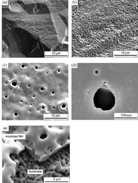
    Figure 1:  SEM images of anodized C.P–Ti, grade 2 in 1M H3PO4
electrolyteduring 1min at (a) 100V, (b) 200V (c) 300V, (d) nanostructure TiO2
and (e) cross section of TiO2 film formed at 300V.
At Ti/Ti oxide interface: Ti ? Ti2+ + 2e- (1)
At Ti oxide/electrolyte interface: 2H2O ? 2O2 -+ 4H+ (2)
2H2O ? O2 (gas) + 4H+ + 4e- (3)
Ti2+ + 2O2 - ? TiO2+ 2e- (4)
Titanium and oxygen ions formed in these reduction–oxidation (redox) reactions are driven through the oxide by an externally applied electric field, resulting in the growth of the oxide.
In addition, Figure 1e illustrates the cross section of titanium oxide film (~ 1μm thick) on CP-Ti, grade 2 which formed at 300V during 1 min in 1M H3PO4.
Chemical composition analysis of anodized surface oxide films
Energy Dispersive X–ray Spectroscopy (EDS) analysis for the anodic surface layer formed atpotentiostatic mode in 1M H3PO4 during 1min at 100, 200, and 300Vis shown in Figure 2. EDS analysis indicates the presence of titanium, oxygen and phosphorus in an anodized oxide film. In addition, by increasing the applied voltage of anodic oxidation treatment, the quantity of oxygen and phosphorus increases, as can be observed in Figure 2. EDS spectra represents 0.53, 2.56, 7.03 (at.%) of phosphorus (P) in the anodic oxide film when treated at 100, 200 and 300V; respectively. Anodic oxidation can incorporate anions from the electrolyte solution into the grown film and it is expected that Phosphorus (P) from the electrolyte solution would grow in all the deposited coatings. Increasing the amount of phosphorus element in the coating can lead to an amorphous nature of the surface oxide film grown during anodizing [21] (Figure 2).
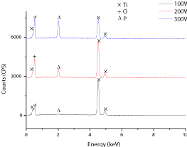
    Figure 2:  EDS analysis of anodic surface layer on C.P–Ti, grade 2 formed in
1M H3PO4electrolyte during 1min for100V, 200V, and 300V.
Phase characterization of anodized surface films
Figure 3 represents Grazing Incidence X–Ray (GIXRD) diffraction patterns of metallic titanium specimens anodized atpotentiostatic mode in 1M H3PO4 during 1min at 100, 200, and 300V anodic voltage; respectively (Figure 3).
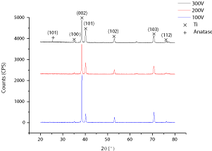
    Figure 3:  Grazing Incidence XRD (GIXRD) patterns of C.P–Ti, grade 2
anodized in 1M H3PO4 electrolyte during 1min at 100, 200, and 300V;
respectively.
The XRD analysis peaks include titanium, amorphous titanium oxide, for which Ti is the main crystal phase in the XRD pattern for all the anodized specimens. Anatase; crystalline Titanium Oxide (TiO2) can just be observed for the sample anodized at 300V anodic applied voltage. The diffraction lines of the anodized surface film obtained at 2θ: 35.94 (2.555A°), 38.442 (2.341A°), 40.171 (2.243A°), 53.005 (1.7262A°), 62.951 (1.4753A°), 70.663 (1.332A°), and 76.221 (1.2481A°) correspond well to the Ti phase (PDF44–1294). One additional peak at 2θ: 25.3198 (3.5169A°) can be assigned to the Anatase phase of TiO2 (PDF89–4203). Titanium dioxide may be presented in both amorphous and crystalline structures, depending on anodic oxidation process parameters. Crystalline titanium oxides i.e. anatase and rutile, possess some exceptional features like photocatalytic behaviour, super hydrophilicity and biocompatible properties, which can be useful for biomedical applications of titanium–based alloys [22]. There may be certain species present in the electrolyte solution, which, when incorporated into the anodic surface oxide films may stabilize the amorphous structure inside the deposited anodic oxide films [23].
Effect of pretreatment and anodizing on surface roughness of C.P–Ti substrate
The influence of surface preparation on surface roughness of metallic Ti samples before and after anodizing atpotentiostatic mode in 1M H3PO4 during 1min is presented in Figure 4. As observed, for four surface preparation methods, the Ti substrates etched using the mixture of aqueous Hydrofluoric and Nitric Acids (HF/HNO3), have the highest mean surface roughness (Ra), while the Ti ones which were ground and polished, have the lowest surface roughness before and after anodizing (Figure 4).
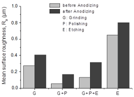
    Figure 4:  Influence of the surface preparation on roughness values of C.P–
Ti, grade 2 specimens before and after the anodic oxidation in 1M H3PO4
electrolyte during 1 min.
Film–substrate adhesion is significantly related to the interface between film and substrate materials. Surface properties of metallic Ti clearly have great influences on the adhesion strength of electrochemically deposited titanium oxide. The adhesion between deposited oxide ceramic and metal has been attributed to mechanical forces, Van der Waal´s forces, chemical bonding by bonding oxides and contracting forces induced through mismatch of expansion coefficients. Van der Waal´sforces include bonding due to electrical dipoles or dispersion effect without accomplishing chemical interaction. Chemical bonds are ordered by oxide layers onto metal substrate material which forms ionic, covalent, or metallic bonds with oxides onto the ceramic. Mechanical inter locking consists of locking one material into pores, cavities, and surface roughness of another material, being the major parameter for adhesion strength of the coating to substrate material [24]. It assumes that the chemical etching pretreatment creates a higher surface roughness than other methods such as grinding or polishing, thereby attaining the adherent interface for titanium oxide–metallic substrate bonding.
Figure 5 represents SEM micrographs of different surface preparation (a) grinding, (b) grinding and polishing, (c) grinding, polishing and etching and (d) etching, which were applied for C.P– Ti ASTM, grade 2 in the present study. The SEM micrographs are in accordance with mean surface roughness, Ra values (Figure 4). Ground and polished C.P–Ti substrates have the lowest surface roughness value, whereas the chemical etched C.P–Ti samples have the highest surface roughness value which is shown in Figure 5.
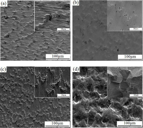
    Figure 5:  SEM micrographs of uncoated C.P–Ti in different surface
preparation: (a) grinding (b) grinding and polishing, (c) grinding, polishing and
etching and (d) etching.
The effect of anodizing on the surface roughness of Commercially– Pure Titanium (C.P–Ti) is represented in Figure 6. It is shown that for all the C.P–Ti specimens, after anodizing, mean surface roughness increased. Additionally, by increasing the applied anodic voltage for anodic oxidation process of Ti specimens, the mean surface roughness increased. Increment of the surface roughness with applied anodic voltage during anodizing treatment could be attributed to the electrical charge resulting in the increase in the titanium oxide film thickness deposited onto the substrate surfaces [20]. Applying a high voltage like 300V, the fusing effect promotes the growth of oxide films onto substrate metals through instantaneous high heat generation during anodic spark growth process [25] (Figure 6).
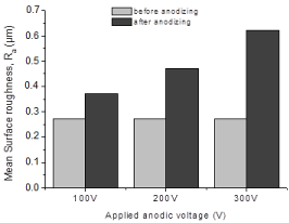
    Figure 6:  Mean surface roughness (Ra variation of ground C.P–Ti, grade 2
specimens before and after anodic oxidation in 1M H3PO4 electrolyte during
1 min.
Conclusion
Nanostructure titanium oxide coatings were deposited onto Commercially–Pure Titanium (C.P–Ti) ASTM grade 2 from H3PO4 electrolyte solution at different applied voltages atpotentiostatic mode through anodic oxidation treatment. Four different surface preparation methods for metallic titanium were applied. Roughness measurement of surface before and after anodic oxidation treatment indicated that chemical etched plate–shaped samples had higher surface roughness than disc–shaped samples. Additionally, roughness measurements indicated that applying higher voltage during anodic oxidation increases surface roughness. Regarding current–time curves during anodizing, a 300Vapplied anodic voltage resulted in greater gas evolution and arc generation than those observed for 100V and 200V, which contributed to the breakdown potential. Scanning Electron Microscopy (SEM) micrographs indicated that by increasing the applied anodic voltage during anodizing, the pore size increases, while the number of pores decreases. Energy Dispersive X– ray Spectroscopy (EDS) analysis confirms the presence of titanium, oxygen and phosphorus in anodized oxide film. Moreover, by increasing the applied voltage of anodic oxidation treatment the quantity of oxygen and phosphorus increases in the grown oxide film.
References
- Vásquez VZ, Ozcan M, Kimpara ET. Evaluation of interface characterization and adhesion of glass ceramics to commercially pure titanium and gold alloy after thermal- and mechanical-loading. Dent Mater. 2009; 25: 221-231.
- Ozcan I, Uysal H. Effects of silicon coating on bond strength of two different titanium ceramic to titanium. Dent Mater. 2005; 21: 773-779.
- Sadeq A, Cai Z, Woody RD, Miller AW. Effects of interfacial variables on ceramic adherence to cast and machined commercially pure titanium. J Prosthet Dent. 2003; 90: 10-17.
- Zinelis S, Tsetsekou A, Papadopoulos T. Thermal expansion and microstructural analysis of experimental metal-ceramic titanium alloys. J Prosthet Dent. 2003; 90: 332-338.
- Setcos JC, Babaei-Mahani A, Silvio LD, Mjör IA, Wilson NH. The safety of nickel containing dental alloys. Dent Mater. 2006; 22: 1163-1168.
- Yan M, Kao CT, Ye JS, Huang TH, Ding SJ. Effect of preoxidation of titanium on the titanium–ceramic bonding. Surf Coat Technol. 2007; 202: 288–293.
- Troia MG, Henriques GE, Mesquita MF, Fragoso WS. The effect of surface modifications on titanium to enable titanium-porcelain bonding. Dent Mater. 2008; 24: 28-33.
- Al Hussaini I, Al Wazzan KA. Effect of surface treatment on bond strength of low-fusing porcelain to commercially pure titanium. J Prosthet Dent. 2005; 94: 350-356.
- Guler A. Surface treatment to increase bond strength. Int J Prosthodont. 2005; 50: 385.
- Gorges R, Meyer S. Surface-functionalization of microstructures by anodic spark oxidation. Proceedings of 6th International Conference on Microreaction Technology (IMRET 6). 2002.
- Kon M, Ishikawa K, Miyamoto Y, Asaoka K. Development of calcium phosphate based functional gradient bioceramics. Biomaterials. 1995; 16: 709-714.
- Liu X, Chu PK, Ding Ch. Surface modification of titanium, titanium alloys, and related materials for biomedical applications. Mat SciEng R. 2004; 47: 49–121.
- Kim DY, Kim M, Kim HE, Koh YH, Kim HW, Jang JH. Formation of hydroxyapatite within porous TiO(2) layer by micro-arc oxidation coupled with electrophoretic deposition. Acta Biomater. 2009; 5: 2196-2205.
- Yerokhin AL, Nie X, Leyland A, Matthews A, Dowey SJ. Plasma electrolysis for surface engineering. Surf Coat Technol. 1999; 122: 73–93.
- Shokouhfar M, Dehghanian C, Baradaran A. Preparation of ceramic coating on Ti substrate by plasma electrolytic oxidation in different electrolytes and evaluation of its corrosion resistance. Appl Surf Sci. 2011; 257: 2617–2624.
- Teng FY, Tai ICh, Wang MW, Wang YJ, Hung Ch Ch, Tseng Ch Ch. The structures, electrochemical and cell performance of titania films formed on titanium by micro–arc oxidation. J Taiwan Ins Chem Eng. 2014; 45: 1331–1337.
- Wang Y, Lei T, Jiang B, Guo L. Growth, microstructure and mechanical properties of microarc oxidation coatings on titanium alloy in phosphate-containing solution. Appl Surf Sci. 2004; 233: 258–267.
- Santos E, Kuromoto NK, Soares GA. Mechanical properties of titania films used as biomaterials. Mat Chem Phys. 2007; 102: 92–97.
- Oh HJ, Leeb JH, Jeong Y, Kim YJ, Chi ChS. Microstructural characterization of biomedical titanium oxide film fabricated by electrochemical method. Surf Coat Technol. 2005; 198: 247–252.
- Park YJ, Shin KH, Song HJ. Effects of anodizing conditions on bond strength of anodically oxidized film to titanium substrate. Appl Surf Sci. 2007; 253: 6013–6018.
- Narayanan R, Seshadri SK. Phosphoric acid anodization of Ti–6Al–4V–Structural and corrosion aspects. Corr Sci. 2007; 49: 542–558.
- Diamanti MV, Pedeferri MP. Effect of anodic oxidation parameters on the titanium oxides formation. CorrSci. 2007; 49: 939–948.
- Habazaki H, Uozumi M, Konno H, Shimizu K, Skeldon P, Thompson GE. Crystallization of anodic titania on titanium and its alloys. CorrSci. 2003; 45: 2063–2073.
- Korkmaz T, Asar V. Comparative evaluation of bond strength of various metal–ceramic restorations. Mat Des. 2009; 30: 445–451.
- Wei CB, Tian XB, Yang SQ, Wang XB, Fu RKY, Chu PK. Anode current effects in plasma electrolytic oxidation. Surf Coat Technol. 2007; 201: 5021–5024.