
Review Article
Ann Materials Sci Eng. 2021; 5(2): 1042.
Design and Simulation of a Broadband Plasmonic Optical Isolator
Olyanasab A1 and Rostami A1,2*
¹Photonics and Nanocrystals Research Lab (PNRL), University of Tabriz, Tabriz, Iran
²SP-EPT Lab, ASEPE Company, Industrial Park of Advanced Technologies, Tabriz, Iran
*Corresponding author: Ali Rostami, Photonics and Nanocrystals Research Lab (PNRL), University of Tabriz, Tabriz, Iran; SP-EPT Lab, ASEPE Company, Industrial Park of Advanced Technologies, Tabriz, 5364196795, Iran
Received: August 25, 2021; Accepted: September 29, 2021; Published: October 06, 2021
Abstract
In this paper, a new approach for optical isolator based on the Plasmonic effect is proposed. Metallic nanoparticles of different sizes are used to realize the proposed idea. Metallic nanoparticles spin-coated on alumina thin layer that is coated on Silicon waveguide. We demonstrated that the proposed idea operates in a broadband spectral range (more than 800nm) as well as back-propagating wave attenuated more than 120dB. The proposed idea can enhance the isolation ratio and also can provide wider bandwidth for isolation. The proposed idea is based on solution process nanotechnology that is simple, low cost, and available.
Keywords: Optical isolator; Broadband isolation; Nanoparticles; Fe Nanoparticles; Isolation ratio
Introduction
An optical isolator or optical diode is a device that restricts light to travel in one direction and allows it to go in another direction. An optical isolator is an essential device in optical communication systems and lasers. It prevents back reflections of light, which could damage other devices. A variety of optical isolators have been proposed over the past years. Rayleigh proposed the first optical isolator which was designed utilizing a Faraday rotator and two polarizers. The origin of non-reciprocity was the Faraday rotator. Because of its magnetically induced anisotropy, the light traveling in two directions along the device rotates differently. By using the polarizers, the light gets blocked in one direction. Rayleigh’s isolator had some major problems. It could not function as a broadband isolator because the rotator depends on wavelength. The second problem is the strong magnetic field, which was used to induce anisotropy to the rotator. Also, it is challenging to make magnets in smaller sizes, which means this device is bulky and could not be integrated with other devices. Additionally, the magnetic field and Verdet constant are temperature-dependent which makes designing this isolator difficult. Strong dependency on the length of the rotator is another difficulty of this isolator. Some of these issues are remained as a problem for fabrication and developing optical isolators. The primary parameters of an optical isolator are isolation ratio, insertion loss, and bandwidth. To gain a high isolation ratio, low insertion loss, and broad bandwidth several works have been done. In most of the structures, iron or garnet was used as the main material and the anisotropy was induced to the iron or garnet by a magnetic field. Table 1 shows the main parameters of the proposed structures. Broad bandwidth and high isolation have not been reached in the presented works and a broadband isolator with high isolation is strongly needed.
    Structure
    Isolation ratio (dB)
    Insertion loss (dB)
    Bandwidth (nm)


    Non-reciprocal coupling [1]
    30
    3
    Single freq.


    Liquid Crystal [2]
    30
    1
    Single freq.


    Tandem phase modulator [3]
    11
    2.3
    Single freq.


    Guided resonance [4]
    25
    0
    Single freq.


    Non-reciprocal optical resonators [5]
    19.5
    18.8
    Single freq.


    Photonic crystal heterojunctions [6]
    22
    12~32
    180nm


    Ring isolator on SOI [7]
    20~80
    -
    Single freq.


    Non-reciprocal Microring resonator [8]
    20
    -
    Single freq.


    Ce:YIG/SOI [9]
    25
    14
    Single freq.


    Atomic vapor in the hyperfine [10]
    30
    0.05
    Single freq.


    MZI [11]
    18
    -
    -


    Stimulated Brillouin scattering [12]
    20
    -
    25


    All-silicon [13]
    28
    -
    Single freq.


    Compact MZI [14]
    11
    -
    Single freq.


    Linear and passive [15]
    6
    -
    50


    Surface Plasmons [16]
    ~800
    -
    Single freq.


    Faraday rotator [17]
    10~40
    -
    50


    CdSe Quantum Dots [18]
    14
    -
    Single freq.


    Ce:YIG on SOI [19]
    32
    -
    Single freq.


    Modulation [20]
    3~5
    -
    40


    Coupled micro resonators [21]
    8
    0
    Single freq.


    Nanorings [22]
    35
    0
    Single freq.


    Cryogenic Faraday Isolator [23]
    30
    -
    Single freq.


    Mode Conversion [24]
    6
    8
    -


    Deposition of Ce:YIG [25]
    13
    7.4
    Single freq.


    Grating coupler [26]
    20
    5.7
    14


    Micro ring [27]
    32
    ~25
    Single freq.


    Nonlinear PT-symmetric lattice [28]
    68.6
    -3.7
    Single freq.


    Four-wave-mixing
    11.3
    19
    2.5


    Canceling phase deviation in MZI [29]
    20
    35
    8


    Four-wave-mixing [30]
    15
    4
    Single freq.


    Microtoroid optomechanical resonator [31]
    10
    ~15
    Single freq.


    Active micorcavity [32]
    16.5
    1.25
    Single freq.


    Tapered metallic grating [33]
    9
    0.5
    ~250


    Microcavity [34]
    6.5~26
    -
    Single freq.


    Four-wave-mixing [35]
    18.3
    7
    2


    Electro-optical emulation [36]
    18.5
    60
    Single freq.


    Microresonator [37]
    78.6
    1
    Single freq.


    Mimicking nonlinear anti-adiabatic [38]
    10
    0
    ~300 (100 THz)
Table 1: Comparison of different methods for the realization of optical isolators.
Some of the new designs are discussed in the following. One of the approaches is using chiral plasmonic-metamaterials. It proposes an achromatic optical isolator. It is based on circular dichroism in metamaterials of twisted chains, which is made of metallic Nanoparticles. Broad bandwidth (approximately 300nm) has been achieved, but the design has a low isolation ratio (less than 5dB). The insertion loss of the proposed isolator is acceptable (nearly 3dB) [39]. Another method is based on a ring resonator. The device consists of a magneto-optical ring resonator with a silver disk embedded in its center. The isolation ratio is reported to reach 20.1dB, and the insertion loss is 0.89dB at the wavelength of 1.38um. The operating bandwidth of the mentioned design is about 10nm, which means it cannot act as a broadband isolator [40]. One of the designs which are compatible with CMOS technology is based on tandem ring modulators. In this scheme, a p-n ring modulator was adopted to reach the isolation function. The maximum isolation ratio of 50dB and insertion loss of 3dB was acquired. The bandwidth of the device is 1.87GHz, which implies it cannot be used as a broadband isolator [41]. One of the trials was based on a magneto-optic Mach-Zehnder interferometer. The design consists of an asymmetric Mach-Zehnder interferometer with a phase shifter. The phase shifter in one of the waveguides is nonreciprocal and is magnetized transversely. In the other waveguide, the phase shifter is reciprocal. Isolation ratio and insertion loss are obtained 50dB and 1dB respectively. The proposed design couldn’t function as a broadband device [42]. One of the structures is based on plasmonic. The design is a multi-layer structure of Si, Al2O3, and Fe. Fe is used as the magneto-optic material to gain non-reciprocal loss. Si is used as a dielectric of the plasmonic structure. And Al2O3 is used to have free carriers and adjust the effective refractive index of the waveguide. High isolation has been attained (800dB/mm) which is acceptable. Because of the high extinction factor of Fe, using it as the metal of the plasmonic structure increase the insertion loss. But it could be compensated by an optical amplifier. Besides, the design could only perform narrowband isolation [43]. In this paper, we demonstrated an isolator with high isolation and ultra-broad bandwidth with a wide incident angle. For the best of the author’s knowledge, it has the broadest bandwidth with the highest isolation ratio and widest incident angle among the reported structures.
Design and Simulation
In this section mathematical modeling and physical description of operation is presented. Figure 1 shows a schematic of the proposed optical isolator.
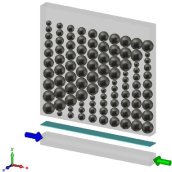
    Figure 1: Schematics of the proposed design. From the bottom: 300nm of
Si, 20nm of Al2O3, and Fe Nanoparticles surrounded by Si. For the forward
direction, port 1 is excited and for the backward direction, port2 is excited.
Figure 1 shows the schematics of our proposed design. It consists of 300nm of Si as substrate, 20nm of Al2O3, and 3000nm of Fe Nanoparticles surrounded by Si. The Nanoparticles have various diameters varying from 160nm to 360nm. Refractive indexes of dielectrics are wavelength-independent. It is determined as 3.5 for Si and 1.74 for Al2O3 at the wavelengths 1200-2000 nm. Permittivity tensor of Fe is described as:

where diagonal elements are the permittivity of Fe without magnetization. Its value for different wavelengths is obtained from the data reported by Ordal (1985). The off-diagonal elements are responsible for the anisotropic feature of Fe which is generated using a magnetic field. It is assumed to equal 36.4 in this paper. iγ is defined as purely real (it doesn’t have an imaginary part), even though having a small imaginary part won’t have any major effect on the result. The simulations are performed by the finite element method. The transmittance of the design is shown in Figure 2. As shown there is a great difference between transmission in the forward and backward direction meaning that the device is an isolator.
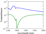
    Figure 2: The transmittance of the proposed design. The blue line shows
the transmittance along the forward direction and the green line shows the
transmittance along the backward direction.
Figure 3a shows the Isolation ratio for this design. The isolation ratio is one of the major parameters to evaluate an isolator. Isolation ratio is defined as a ratio of the transmittance in the forward direction to the transmittance in the backward direction:
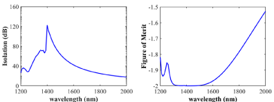
Figure 3: a) Isolation ratio of the plasmonic isolator utilizing Nanoparticles. b) Figure of merit of the proposed design.
An optical isolator is as functioning as its great isolation ratio. The isolation ratio of our design reaches its maximum value at the wavelength of 1400nm with a value of 120dB (33333dB/mm) and its minimum value is 20dB (5555dB/mm) for the wavelength of 2000nm. As discussed before, the generated anisotropy is assumed to compensate for the loss of wave in one direction and its value is equal to the imaginary part of permittivity which is responsible for the loss. If the generated anisotropy is different than the assumed value, the maximum isolation will occur in other wavelengths. The performance of the isolator won’t be affected, nonetheless, the value of isolation ratio and insertion loss would change a bit. The figure of merit for optical isolator could be defined as the ratio of optical isolation to average loss:
If an ideal isolator is supposed, the loss mechanism in the forward direction will be zero, and loss in the backward direction would be infinite. Hence the value of FoM for the ideal isolator is -2. Figure 3b shows the figure of merit for the isolator discussed in this paper. For a considerably large range of the bandwidth, the value of FoM equals -2 which this part includes 1310nm and 1550nm wavelengths. For higher isolations, two or more periods of this structure could be used. Simulation shows that isolation of a structure with two periods is twice as high as isolation of one period. In this case, FoM is closer to its ideal form, and the range in which FoM equals -2 is larger than it is in one period.
In addition to the isolation ratio and figure of merit, the propagating wave should have a proper shape across the device. Figure 4a and 4b) shows the magnetic field along the Z direction for λ=1310nm and 1550nm which are standard wavelengths for optical communications. As shown, in both wavelengths Hz in the forward direction has a proper shape.
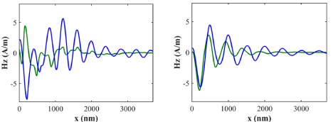
    Figure 4: The magnetic field along Z direction a) λ=1310nm. b) λ=1550. The blue line shows Hz in the forward direction and the green line shows Hz in the
backward direction.
One of the problems is due to the small size of the isolator, it is hard to excite a port with a specific or with a narrow range of incident angles. This problem is reported in some of the works with an incident angle range as narrow as 0.1 degrees [44]. Figure 5 shows S parameters and Figure 6 shows the isolation ratio for different incident angles. It is clear from these figures that for a wide range, the incident angle won’t affect the performance of the isolator a lot.
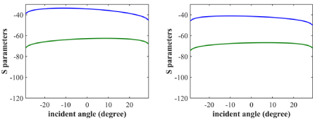
Figure 5: S parameters for different incident angles. a) λ=1310nm, b) λ=1550nm. The blue line is S21 and the green line is S12.
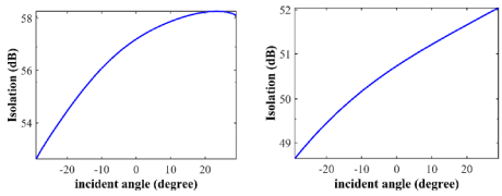
Figure 6: Isolation ratio for different incident angles. a) λ=1310nm. b) λ=1550nm.
For any optical device, it is essential to prove that light is coupled in the waveguide. Mode analysis is commonly used to show this feature. Figure 7 shows modes for 2 important wavelengths of 1310nm and 1550nm. Four cut lines are defined to show the light is coupled properly along the waveguide. The spike shown in the figures is the boundary between Al2O3 and Fe Nanoparticles which is the plasmonic waveguide.
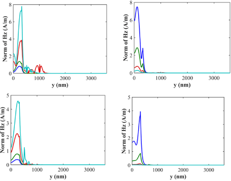
    Figure 7: Modes of light along the waveguide. a) λ=1310nm in forward direction. b) λ=1310nm in backward direction. c) λ=1550nm in the forward direction. d)
λ=1550nm in backward direction. The cyanide, red, green, and blue lines are for x=555nm, 1295nm, 2405nm, and 3145nm respectively.
As discussed before, the major use of isolators is to prevent unwanted reflection of light, so isolators need to have a small value of reflection. Figure 8 shows the value of reflectance for different wavelengths. Reflectance is nearly zero for all of the bandwidth range. Figure 9 shows reflectance for different incident angles which prove reflectance is nearly zero for a large range of incident angles.
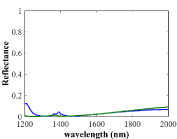
Figure 8: Reflectance for different Wavelengths.
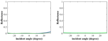
    Figure 9: Reflectance for different incident angles. a) λ=1310nm. b) λ=1550nm. The blue line indicates forward direction and the green line indicates backward
direction.
Conclusion
A broadband isolator with high isolation ratio and a wide incident angle is proposed and simulated. It is based on a Plasmonic waveguide with induced anisotropy. The structure consists of 3 layers Si, Al2O3, and Nanoparticles. The Nanoparticles have different diameters and are made of Fe. The bandwidth of 800nm and maximum isolation of 120dB is gained. For higher isolations, two or more periods of the structure could be used in cascade. It is shown by simulation that in this case, total isolation would be multiplied. For further researches, it is suggested to use other MO substances instead of Fe. Some of these substances have lesser extinction factors than Fe. So replacing Fe with these matters may decrease insertion loss. Thus it would increase the performance of the device. Another approach could be using other ways to obtain non- reciprocity such as non-linear waveguides or materials with constant magnetization. An increasing number of Nanoparticles may have wider bandwidth and choosing the proper radius may adjust the range of the bandwidth to specific applications.
References
- Montoya J, et al. Surface plasmon isolator based on nonreciprocal coupling. Journal of Applied Physics. 2009; 106: 023108-023108.
- Huang Z-D, et al. A Liquid Crystal Tunable Wavelength-Interleaved Isolator with Flat Spectral Response. Journal of Light wave Technology. 2010; 28: 2890-2896.
- Doerr CR, N Dupuis and L Zhang. Optical isolator using two tandem phase modulators. Optics Letters. 2011; 36: 4293-4295.
- Fang K, et al. Ultracompact nonreciprocal optical isolator based on guided resonance in a magneto-optical photonic crystal slab. Optics Letters. 2011; 36: 4254-4256.
- Bi L, et al. On-chip optical isolation in monolithically integrated non-reciprocal optical resonators. Nature Photonics. 2011; 5: 758-762.
- Wang C, C-Z Zhou and Z-Y Li. On-chip optical diode based on silicon photonic crystal heterojunctions. Optics Express. 2011; 19: 26948-26955.
- Pintus P, M-C Tien and J Bowers. Design of Magneto-Optical Ring Isolator on SOI Based on the Finite-Element Method. Photonics Technology Letters, IEEE. 2011; 23: 1670-1672.
- Zhu H and C Jiang. Optical Isolation Based on Nonreciprocal Micro-Ring Resonator. Journal of Light wave Technology. 2011; 29: 1647-1651.
- Ghosh S, et al. Ce: YIG/Silicon-on-Insulator waveguide optical isolator realized by adhesive bonding. Optics Express. 2012; 20: 1839-1848.
- Weller L, et al. Optical isolator using an atomic vapor in the hyperfine Paschen – Back regime. Optics Letters. 2012; 37: 3405-3407.
- Shoji Y, et al. MZI optical isolator with Si-wire waveguides by surfaceactivated direct bonding. Optics Express. 2012; 20: 18440-18448.
- Poulton CG, et al. Design for broadband on-chip isolator using stimulated Brillouin scattering in dispersion-engineered chalcogenide waveguides. Optics Express. 2012; 20: 21235-21246.
- Fan L, et al. An All-Silicon Passive Optical Diode. Science (New York, N.Y). 2011; 335: 447-450.
- Ghosh S, et al. Compact Mach-Zehnder interferometer Ce:YIG/SOI optical isolators. IEEE Photonics Technology Letters. 2012; 24: 1653-1656.
- Wang C, X-L Zhong and Z-Y Li. Linear and passive silicon optical isolator. Scientific Reports. 2012; 2: 674.
- Zayets V, et al. Optical Isolator Utilizing Surface Plasmons. Materials. 2012; 5: 857-871.
- Berent M, A Rangelov and N Vitanov. Broadband Faraday Isolator. Journal of the Optical Society of America A. 2013; 30: 149.
- Ju S, et al. Demonstration of All-Optical Fiber Isolator Based on a CdSe Quantum Dots Doped Optical Fiber Operating at 660nm. Journal of Lightwave Technology. 2013; 31: 3093-3098.
- Ghosh S, et al. Optical Isolator for TE Polarized Light Realized by Adhesive Bonding of Ce:YIG on Silicon-on-Insulator Waveguide Circuits. Photonics Journal, IEEE. 2013; 5: 6601108-6601108.
- Doerr CR, L Chen and D Vermeulen. Silicon photonics broadband modulationbased isolator. Optics Express. 2014; 22: 4493-4498.
- Chang L, et al. Parity-time symmetry and variable optical isolation in activepassive- coupled microresonators. Nature Photonics. 2014; 8: 524-529.
- Sounas DL and A Alù. Angular-Momentum-Biased Nanorings To Realize Magnetic-Free Integrated Optical Isolation. ACS Photonics. 2014; 1: 198-204.
- Starobor A, et al. Cryogenic Faraday Isolator Based on TGG Ceramics. IEEE Journal of Quantum Electronics. 2014: 50: 749-754.
- Aroua W, et al. Mode Converter Optical Isolator Based on Dual Negative Refraction Photonic Crystal. Journal of Quantum Electronics, IEEE. 2014; 50: 633-638.
- Sun XY, et al. Single-Step Deposition of Cerium-Substituted Yttrium Iron Garnet for Monolithic On-Chip Optical Isolation. ACS Photonics. 2015; 2: 856-863.
- Heck M. Grating Coupler Enabled Optical Isolators and Circulators for Photonic Integrated Circuits. IEEE Journal of Selected Topics in Quantum Electronics. 2015; 21: 1-9.
- Huang D, et al. Electrically Driven and Thermally Tunable Integrated Optical Isolators for Silicon Photonics. IEEE Journal of Selected Topics in Quantum Electronics. 2016; 22: 1-1.
- Nazari F and M Moravvej-Farshi. Multi-Channel Optical Isolator Based on Nonlinear Triangular Parity Time Symmetric Lattice. IEEE Journal of Quantum Electronics. 2016; 52: 6100207:1-7.
- Furuya K, et al. Athermal Operation of a Waveguide Optical Isolator Based on Canceling Phase Deviations in a Mach-Zehnder Interferometer. Journal of Lightwave Technology. 2015; 34: 1699-1705.
- Hua S, et al. Demonstration of a chip-based optical isolator with parametric amplification. Nature Communications. 2016; 7: 13657.
- Ruesink F, et al. Nonreciprocity and magnetic-free isolation based on optomechanical interactions. Nature Communications. 2016; 7: 13662.
- Jiang X, et al. On-Chip Optical Nonreciprocity Using an Active Microcavity. Scientific Reports. 2016; 6: 38972.
- Tang B, et al. Broadband asymmetric light transmission through tapered metallic gratings at visible frequencies. Scientific Reports. 2016; 6: 39166.
- Zheng Y, et al. Optically induced transparency in a micro-cavity. Light: Science & Applications. 2016; 5: e16072-e16072.
- Wang K, et al. Silicon Integrated Optical Isolator with Dynamic Non- Reciprocity. IEEE Photonics Technology Letters. 2017; 29: 1261-1264.
- Qin C, et al. Single-Tone Optical Frequency Shifting and Nonmagnetic Optical Isolation by Electro-Optical Emulation of a Rotating Half-Wave Plate in a Traveling-Wave Lithium Niobate Waveguide. IEEE Photonics Journal. 2017; 9: 1-1.
- Kim J, S Kim and G Bahl. Complete linear optical isolation at the microscale with ultralow loss. Scientific Reports. 2017; 7: 1647.
- Choi Y, et al. Extremely broadband, on-chip optical nonreciprocity enabled by mimicking nonlinear anti-adiabatic quantum jumps near exceptional points. Nature Communications. 2017; 8: 14154.
- Rangelov A, S Droulias and V Yannopapas. A Broadband Optical Isolator Based On Chiral Plasmonic-Metamaterial Design. Progress in Electromagnetics Research M. 2019; 81: 67-73.
- Chen J, et al. Nonreciprocal isolator based on a plasmonic magneto-optical resonator. Optics Communications. 2019: 459.
- Jain A, S Arafin and S Dwivedi. CMOS Compatible Optical Isolator with Tandem Ring Modulators. 2019.
- Dehaghani N and A Alizadeh. Design, simulation and optimization of a nonreciprocal guided-wave optical isolator based on Mach-Zehnder interferometer. Journal of Physics Communications. 2019; 3.
- Zayets V, et al. Optical Isolator Utilizing Surface Plasmons. Materials. 2012; 5: 857-871.
- Kaihara T, et al. Magnetic field control and wavelength tunability of SPP excitations using Al2O3/SiO2/Fe structures. Applied Physics Letters. 2016; 109: 111102.