Research Article
Austin J Nanomed Nanotechnol. 2014;2(2): 1015.
Laser-Assisted Nanofabrication of Carbon Nanostructures
Yun Shen Zhou*
Department of Electrical Engineering, University of Nebraska-Lincoln, USA
*Corresponding author: Yun Shen Zhou, Department of Electrical Engineering, University of Nebraska - Lincoln, Lincoln, NE 68588-0511
Received: January 06, 2013; Accepted: March 17, 2014; Published: March 24, 2014
Abstract
Unique features of lasers, such as spatial and temporal coherence, low divergence, high power density and monochromaticity, endorse a broad spectrum of applications in fabricating nanostructured materials. Based on laser-material interactions, such as localized heating, optical near–field effect, ablation, and resonant excitation, a number of laser–assisted techniques, laser exfoliation, laser direct writing, laser–assisted chemical vapor deposition, and laser–assisted combustion synthesis, were developed in our group for fabricating carbon nanostructures of different dimensionalities, including two–dimensional graphene, one dimensional carbon nanotubes, and zero–dimensional carbon nanoonions.
Keyword: Laser, Carbon nanostructures, Laser–assisted chemical vapor deposition, Laser–assisted combustion synthesis, Laser exfoliation, Laser direct writing, Graphene, Carbon nanotube and Carbon nanoonion.
Introduction
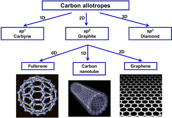
Due to its versatile bonding and atomic arrangements, the element carbon is capable of forming multiple allotropes, as shown in (Figure 1), and exhibits diverse properties [1]. The discovery of buckminsterfullerene (C60) [2] opened a magic door towards the fairyland of carbon nanostructures followed by consecutive discoveries of fullerenes, [2–6] carbon nanotubes (CNTs), [7] and graphene,[8, 9] which are then recognized as new carbon allotropes. Based on their dimensionalities, the new carbon nanostructures can be classified into three major categories, including zero–dimensional (0D) fullerenes and carbon nanoonions (CNOs), one dimensional (1D) CNTs and carbon nanoscrolls (CNSs), and two–dimensional (2D) graphene.
Figure 1: Carbon family tree showing known carbon allotropes.
The carbon nanostructures not only provide ideal platforms for enriching fundamental understanding at nanoscale, but also inspiring ground–breaking breakthroughs in practical applications due to their diverse while remarkable properties [10–46]. The carbon nanostructures have purged several consecutive heat–waves in both scientific and engineering communities, and exerted significant impacts in almost every scientific and engineering field [10–46]. A broad spectrum of applications has been investigated to renovate traditional applications and motivate innovative products [10–46]. A number of start–up companies have emerged developing nanocarbonbased products. It is expected that the advancements of the carbon nanostructures were able to provide solutions satisfying the world’s hunger in various fields and yielding affordable products in daily life. Therefore, controlled fabrication of the carbon nanostructures is required to meet the steadily growing market.
The unique properties of lasers offer distinctive capabilities in nanofabrication [47, 48]. It has been well known that the unique lasermaterial interactions can lead to permanent changes in materials which are not easily achievable through other means [47, 48]. When projected onto material surfaces, laser irradiation can accurately deliver very low (˜ mW) to extremely high (˜ 100 kW) large power into confined regions with a precise spot size⁄dimension and spatial⁄ temporal distribution, and causes a variety of effects, including ablation, shockwave peening, photo–thermal and photo–chemical processes [47, 48]. A wide spectrum of laser wavelengths makes it possible to achieve purposeful energy delivery to a target material through resonant excitation by providing photons of matching energy to interact with the target material, such as laser–induced bond breaking and bond–selective chemical reactions [47, 48]. Easy manipulation of laser beams stimulates the development on the mask–free direct laser writing of nanostructures. Extremely intense energy delivery through laser beams results in a rapid thermal process at the laser focal point, which provides an incomparable cold–wall rapid thermal processing technique. Polarization–dependent lasermaterial interactions provide unique feasibilities in the controllable fabrication of nanostructures, such as tip–induced optical near field enhancement. As a result, a wide variety of laser–based synthetic strategies have been developed in fabricating nano–materials and structures. Since the very beginning of nano–science and technology, lasers have played a significant role in fabricating and producing desired nanomaterials and structures. For example, the laser ablation has been established as one of the most successful synthetic methodsin the scalable production of fullerenes and CNTs, [49–55] and is currently widely adopted in commercial production.
In this review article, an overview of laser–based synthetic techniques developed in the authors’ research team, Laser–Assisted Nano–Engineering (LANE) Lab at the University of Nebraska– Lincoln (UNL), for fabricating carbon nanostructures is presented,including 1) laser direct writing graphene patterns,[56, 57] 2) production of graphene via laser–assisted exfoliation of graphite,[58, 59] 3) laser–assisted controlled growth and integration of carbon nanotubes,[60–65] and 4) laser–assisted scalable production of carbon nanoonions [66].
Laser–Assisted Fabrication of Two–Dimensional Graphene
Since the first experimental discovery of graphene in 2004, [8] graphene quickly captured extensive attention from scientists and engineers due to its importance in fundamental science, remarkable properties, and a broad range of promising applications [9, 20, 23, 25– 27, 30, 35, 36,67, 68]. Due to its 2D planar dimensionality, graphene is relatively convenient to manipulate and highly compatible with current state–of–the–art complementary metal-oxide- semiconductor (CMOS) techniques. Its exceptional optical, electrical and thermal properties make graphene an ideal candidate for flexible and transparent electronics, such as e–paper, flexible displays, interactive touch panels, solar cells, and transparent electrodes [9, 20, 23, 25– 27,30, 35, 36, 67, 68]. Conventional approaches for growing graphene include mechanical exfoliation, [8] high–temperature annealing of SiC, [69,70] chemical vapour deposition
(CVD), [30, 71–73] solid–state carbon transformation, [74] and reduced graphene oxide [75–77]. Graphene obtained from different synthetic methods demonstrates different properties, suitable for diverse applications. In LANE, we developed several laser–based techniques for growing graphene, including 1) laser exfoliation of highly oriented pyrolytic graphite (HOPG), [58, 59] and 2) laser direct writing of graphene [56, 57].
Although the CVD method can achieve scalable growth of graphene using a roll–to–roll method, fabrication of graphene patterns, which are required developing grapheme–based functional devices, is a still a multistep time–consuming and costly process requiring expensive lithographic processes. Therefore, a convenient approach is required to achieve fast, scalable and affordable production of graphene patterns. In LANE, we developed a laser–assisted CVD (LCVD) method and successfully achieved direct writing graphene patterns using a laser as the pen and gaseous hydrocarbon precursors as the ink [56, 57]. Line–shaped graphene ribbons of controlled widths and lengths were precisely fabricated on a Ni foil without extra annealing and lithographic patterning procedures. Transparent interconnections connecting multiple electrodes were fabricated by transferring the graphene ribbons onto SiO2⁄Si substrates containing pre–deposited electrodes. The localized laser heating results in a rapid thermal process at the laser beam focal point. Graphene patterns could be fabricated at a scanning speed up to 200 μm⁄s, which is much faster and more convenient than a traditional fabrication approach. Direct writing graphene patterns using the LCVD methodexpands the capability of CVD approaches in rapid and controllable fabrication of graphene for a wide range of application.
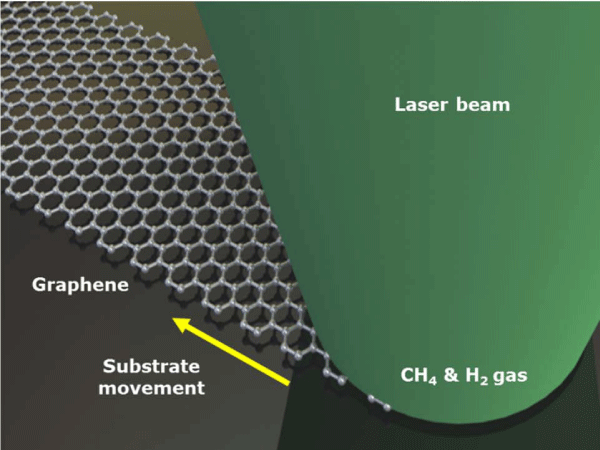
(Figure 2) demonstrates a schematic diagram of laser direct writing graphene on a nickel (Ni) foil using the LCVD method, in which a continuous wave laser (Coherent G5, λ = 532 nm) was used as the pen and a methane–hydrogen gas mixture as the ink. The graphene growth process was performed in an environmental chamber with a base pressure of 10–3 torr. The laser beam was normally projected onto the Ni foil with a spot diameter of 20 μm. A motorized stage was used to move the Ni foil precisely following the designed pattern for writing graphene patterns. The fabricated graphene patterns can be transferred onto required substrates by using poly (methyl methacrylate) (PMMA) stamps [56, 57].
Figure 2: A schematic diagram of laser direct writing graphene.
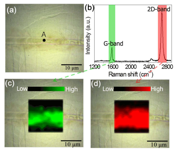
(Figure 3a) shows an optical micrograph of a line–shaped graphene ribbon on a Ni foil as prepared using the LCVD method. Rippled edges on the graphene ribbon were ascribed to the difference between the thermal expansion coefficients of Ni and graphene. (Figure 3b) shows a Raman spectrum of spot–A in (Figure 3a), clearly indicating the existence of monolayer graphene. Both symmetric 2D–band at 2691 cm–1 and a high 2D⁄G band ratio (around 3 – 4) confirm the existence of monolayer graphene. Invisible D–band demonstrates the high quality of the as grown graphene. (Figures 3c and 3d) show the Raman mapping of the graphene ribbon using Gband (green) and 2D–band (red), respectively. Sharp edges between the graphene ribbon and surrounding areas are observed, demonstrating precise position control in direct writing graphene. Relatively uniform Raman intensity distribution in both G– and 2D–bands indicates the homogeneity of the graphene ribbons.
Figure 3: (a) Optical micrograph of a graphene pattern on a nickel foil; (b) corresponding. Raman spectrum at point-A. Raman intensity mapping of (c) G-band (1582 cm-1) and (d) 2D-band (2691 cm-1) (wavelength = 514.5 nm).
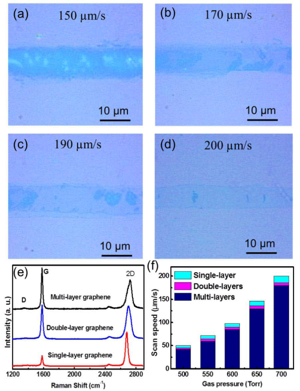
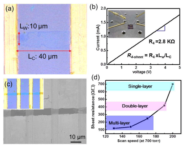
The number of graphene layers could be precisely controlled by tuning the scan speed of the laser beam. (Figures 4a to 4d) show optical micrographs of the graphene ribbons fabricated on SiO2⁄ Si substrates with respect to different laser scan speeds. Graphene of different number of layers, single, double, and multi–layer, were obtained at different scanning speed. Generally speaking, the slower the laser scanning speed, the more the layer number is. (Figure 3e) shows the Raman spectra of the graphene ribbons fabricated at different laser scan speeds. (Figure 3f) shows the control of graphene layers with respect to the gas pressures and laser scan speeds.
Figure 4: Optical micrographs of (a) transferred, (b) multilayer, (c) doublelayer, and (d) single-layer graphene ribbons on SiO2⁄Si surfaces. (e) Typical Raman spectra of multilayer, double-layer, and singlelayer graphene. (f) Fabrication window of different layers of graphene with respect to the gas pressures and scan speeds.
(Figure 5a) shows a typical optical micrograph of a highly transparent graphene ribbon transferred onto a gold electrode. The sheet resistance of the monolayer graphene ribbon was measured to be 700 O⁄sq, as shown in (Figure 5b & Figure 5c) shows both optical and SEM micrographs of a multilayer graphene ribbon transferred onto gold electrodes. Sheet resistance of graphene ribbons obtained at different laser scan speeds was recorded, as shown in (Figure 5d).
Figure 5: (a) Optical micrograph of a transferred single-layer graphene on gold electrodes. (b) I-V characteristic of the single-layer graphene pattern. (c) SEM micrograph of a multilayer graphene pattern. Inset shows an optical micrograph of the multilayer graphene pattern. (d) Sheet resistances of a graphene pattern with respect to the scan speeds.
Due to its versatile potential applications, large quantity of graphene is demanded, therefore requiring an affordable and scalable production technique. As the first successful graphene fabrication approach, mechanical exfoliation from highly ordered pyrolytic graphite (HOPG) has been demonstrated to be the most straightforward and simple method [8, 9]. However, the low throughput makes this method only applicable for lab use. The LANE developed a pulsed–laser exfoliation technique producing graphene directly from HOPG [58, 59]. By using a pulsed Nd: YAG laser (wavelength = 532 nm), exfoliation of HOPG can be performed either in vacuum or in liquid [58, 59]. Multi–layer graphene was obtained. It was found out that the formation of graphene was achieved within a laser fluence window from 1.0 to 10.0 J ⁄cm2. The formation of graphene is ascribed to the immediate compression and expansion of the HOPG, which leads to the exfoliation of graphene sheets from the layered structure of HOPG [58, 59].
Laser–Assisted Fabrication of One–Dimensional Carbon Nanotubes
Discovery of CNTs has brought a revolutionary vision to the scientists and engineers due to their unique structures and extraordinary properties [19, 24,32,46,78,79]. A wide spectrum of CNT based applications have been proposed and investigated. CNTs have been envisioned as one of the most promising candidates for fabricating next–generation electronic devices [19,24,32,46,78,79]. Extensive investigations were already made in fabricating CNTbased components and devices, such as transistors, logic gates, interconnects, sensors and detectors [13–18, 29,33, 34,38–40,43,44,80– 87]. Extensive and practical applications of CNTs in the field of electronics and devices require precisely controlled growth and integration of CNTs. Several critical topics, including where it starts, where it goes, alignment direction, stable wiring, and electrical types, have to be addressed to meet the challenges. Ideally, it is desired that CNTs of determined electrical types were precisely wired between electrodes with stable contacts for device fabrication [88–93]. However, such precise control is extremely challenging due to the ultra–tiny size of the CNTs, high–resolution nanoscale positioning, and subtle structure diversity [88–93].
Tremendous efforts have been made to solve the challenges. Techniques, such as chemical vapour deposition, [94–96] scanningprobe– microscope–assisted patterning, [89,97,98] template directed assembly, [99–101] and dielectrophoresis deposition, [102–105] have been investigated trying to achieve controlled integration of CNTs. However, existing drawbacks (such as high processing temperature, slow processing speed, coarse control, liquid phase processing⁄ contamination, low reliability, low yield and high cost) of individual approaches make it difficult to develop a high–performance–ondemand approach for fabricating CNT–based devices.
To address the challenges, a series of laser–assisted techniques were developed in LANE, including optically controlled parallel integration of CNTs into pre–designed micro⁄nanoarchitectures in a single step, [60,61] selective removal of metallic CNTs through laser irradiation, [64] and growing diameter–modulated singlewalled CNTs [63]. Based on the laser assisted techniques developed, investigators in LANE successfully fabricated plasmonicenhanced CNT infrared bolometers [62].
Optically Controlled Parallel Integration of CNTs
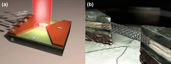
Optically controlled parallel integration of CNTs was achieved through a LCVD method, [60,61] as shown in (Figure 6). CNTs were wired between electrodes pre–patterned on SiO2⁄Si substrates. Ultrasharp electrode tips were fabricated using focused–ion–beam (FIB) milling technique and used as optical antennas to focus and enhance optical fields within the laser irradiated regions. A continuous–wave (CW) CO2 laser (wavelength = 10.6 μm) was used to irradiate the patterned substrates. The laser beam has a polarization horizontally linearized. The SiO2⁄Si substrate was heated up to 500 °C, which is almost 200 °C lower than a conventional LCVD process, before feeding the gaseous precursors. A gas mixture of acetylene (C2H2) and anhydrous ammonia (NH3) was used as precursor for growing CNTs. (Figure 6b) shows a schematic structure of a CNT–integrated bridge structure.
Figure 6: (a) A schematic diagram of the LCVD fabrication process for growing CNTs, and (b) a schematic diagram of a CNT-integrated bridge structure.
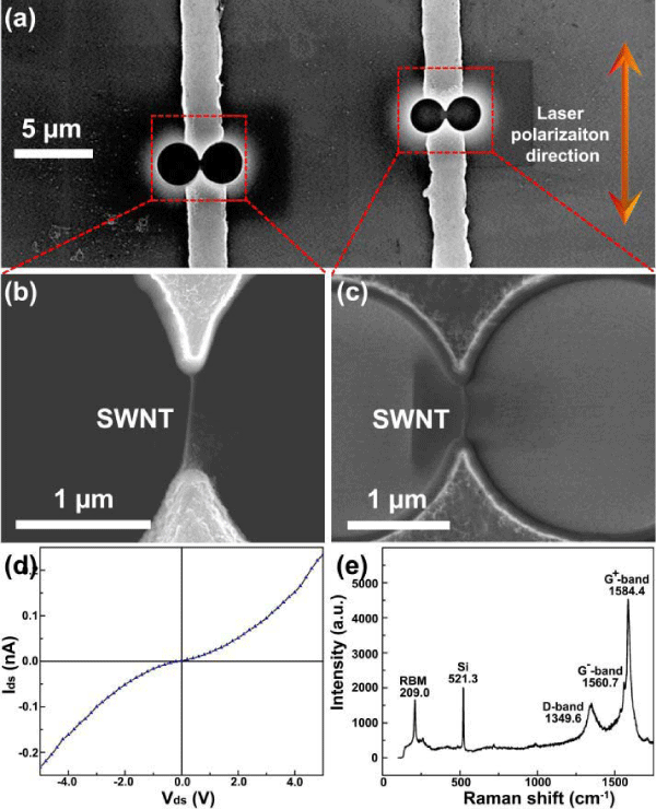
(Figures 7a and 7b) show a top–view and side–view, respectively,of a typical CNT–bridge structure. Typical Raman spectrum of the CNT–bridge, (Figure 7c), shows a sharp radial breathing mode (RBM) shift at 207.6 cm–1, a Lorentzian line–shaped G– band at 1567.8 cm–1, and a strong G band at 1591.5 cm–1 indicating the existence of singlewalled semiconducting CNTs (s–CNTs) with an estimated diameter of 1.2 nm [106–108]. Simultaneous integration of CNTs into multiple sites is demonstrated in (Figure 8a, Figures 8b and 8c) exhibit zoomed images of the squared regions in (Figure 8a) and clearly show precisely integrated CNTs between each pair of tip–shaped electrodes. Only one CNT was observed between each pair of the electrodes. All CNTs are rooted at the electrode tips, indicating a site selective growth mode. The CNT–bridge structures show a nonlinear Ids-Vds curve, as shown in (Figure 8d). In the Raman spectrum, as shown in (Figure 8e), a sharp RBM Raman shift at 209.9 cm–1 and a Lorentzian line–shaped G– band are observed, and indicate the growth of s–CNTs with an estimated diameter of 1.19 nm [106–108].
Figure 7: Typical SEM images of a CNT-bridge structure: (a) top-view and (b) side-view, and (c) corresponding Raman spectrum of the CNTs.
Figure 8: (a) An SEM image showing an electrode pattern containing two pairs of electrodes; (b) and (c) SEM images of the squared regions in (a), showing the CNT- bridge structures; (d) I-V measurement of the device; and (e) Raman spectrum of the CNTs.
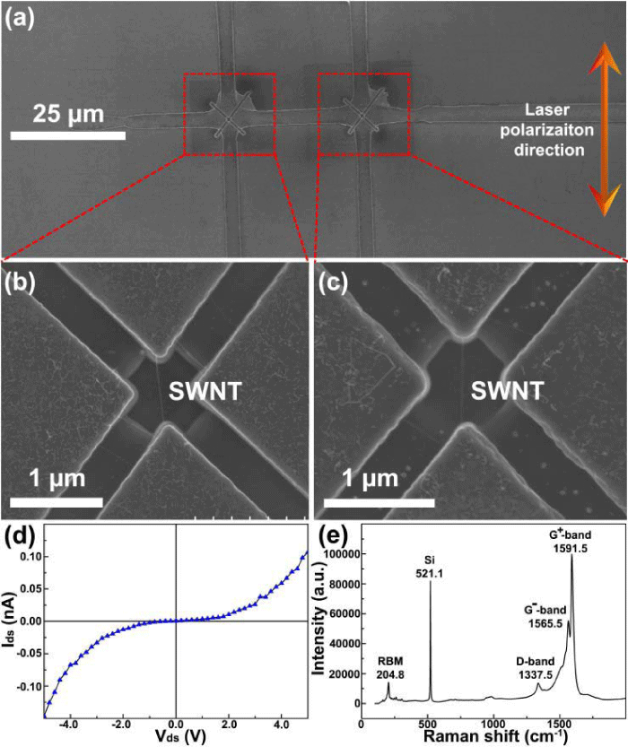
It was found that laser polarization played a significantly role in the selective growth of CNTs. As shown in (Figure 9a to 9c), crossshaped electrodes were fabricated. It is well known that optical nearfield enhancement is a function of wavelength, material, geometry and polarization of the exciting light field [109, 110]. Under the same circumstance, the field–enhancement factor is in reverse proportion to the tip angle. The laser polarization was set to be parallel to one pair of the tips, as shown in (Figure 9a). To exclude the influence from the electrical field, no external electrical field was used. CNTs were precisely wired between tips parallel to the laser polarization as shown in (Figures 9b and 9c). Growth of CNTs showed obvious selectivity on position and orientation between the electrode tips parallel to the laser polarization. A similar nonlinear Ids-Vds curve was observed as shown in (Figure 9d). The sharp RBM peak at 204.8 cm–1, (Figure 9e), indicated the growth of CNTs with a diameter of 1.21 nm [106–108].The G– band at 1565.5 cm–1 showed a Lorentzian line shape, a characteristic of s–CNTs [106–108].
Figure 9: (a) An SEM image showing the electrode pattern containing cross-shaped electrodes; (b) and (c) SEM images of the squared regions in (a), showing the CNTintegrated bridge structures; (d) I-V measurement of the device; and (e) Raman spectrum of the CNTs.
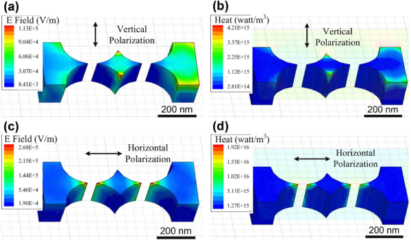
It is well known that sharp metallic tips can be used to enhance the electromagnetic field at nanoscale tip regions and result in an enhanced localized heating at the apexes of the metallic tips [109,110]. Numerical simulations, using the high frequency structure simulator (HFSS, Ansoft), were conducted. Laser beams of different polarization directions were used separately in the simulation, perpendicular (Figures 10a and 10b) and parallel (Figures 10c and 10d) to the electrode alignment. (Figures 10a and 10c) show the electrical field distribution in the metallic tips under laser irradiation of different polarization directions. Significant enhancement of the local electrical field is observed at the tips parallel to the laser polarization, almost tenfold stronger than that of the rest of the electrodes. Since a changing electromagnetic field generates an eddy current, the enhanced high–frequency E–field at the tips results in a significantly enhanced local eddy current and yields an enhanced localized heating at the nanoscale. (Figures 10b and 10d) show the heat distributions in the metallic tips under laser irradiation of different polarization directions. The local heating enhancement reaches the maximum at the tips parallel to the laser polarization, almost one order of magnitude larger than that of the rest of the electrodes. Therefore, a significant temperature increase at the tips is induced by the optical near–field effects. The simulation results confirm the hottest spots at the electrode tips parallel to the laser polarization, resulting in the selective growth of CNTs parallel to the laser polarization, (Figures 9b and 9c). Therefore, the CNT growth control is ascribed to the selective heating of electrode tips caused by the optical near–field effect, which is influenced by the laser beam polarization.
Figure 10: Electrical field distribution (a) and heat distribution (b) within the electrodes with the laser beam polarization normal to the electrode tip pair; electrical field distribution (c) and heat distribution (d) within the electrodes with the laser beam polarization parallel to the electrode tip pair.
Selective Removal of Metallic Cnts through Laser Irradiation
LANE achieved selective removal of metallic CNTs (m–CNTs) through a post–growth laser processing [64]. An optical parametric oscillator (OPO) wavelength tunable laser (Continuum, Panther ® EX) was used as the laser irradiation source, which provides laser emission ranging from 215 to 2550 nm. Pulsed laser beams with a wavelength of 2 μm (power density of 1.8 MW⁄mm2.) were used for the selective removal process. Laser beams of shorter wavelengths could cause obvious damage to both s– and m–CNTs due to the highenergy photons. Wavelengths larger than 2 μm were not investigated due to the sharp drop of the output power for wavelength over 2 μm from the OPO laser.
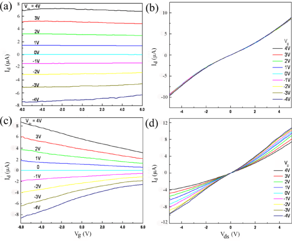
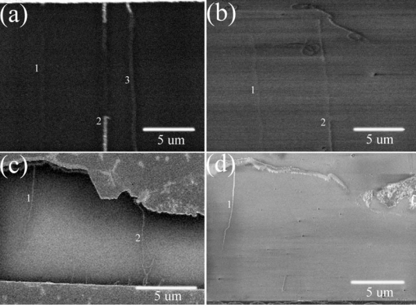
Well aligned CNT arrays between parallel electrodes were fabricated, resembling a function of CNT–based field–effect transistors (CNT–FETs). It is well known that m–CNTs and s–CNTs show distinctly different electrical transport behaviours. CNT arrays containing m–CNTs exhibit linear electric transport features independent of Vg. (Figures 11a and 11b) show the Id-Vg and Id- Vds curves of a CNT array before laser irradiation with obvious existence of m–CNTs confirmed by the linear curves and absence of Vg dependence. The CNT array was irradiated using the OPO laser. After the laser irradiation, (Figures 11c and 11d), I-V curves show nonlinear semiconducting behavior and obvious Vg dependence. SEM images of the same sample were taken before and after the laser irradiation to compare the physical changes of the CNTs, as shown in (Figure 12). All CNTs were labeled before laser irradiation. Afterlaser irradiation, CNTs 3 and 2 are removed in (Figures 12b and 12d), respectively.
Figure 11: Id-Vg and Id-Vds curves of a typical CNT-FET sample before, (a) and (b), and after, (c) and (d), laser irradiation, respectively.
Figure 12: SEM images of the CNT arrays before, (a) and (c), and after, (b) and (d), laser irradiation. Each number marks to the same CNT before and after laser irradiation.
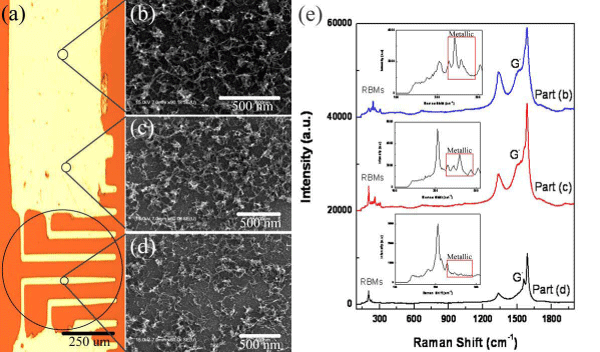
Raman spectroscopic investigations were carried out to verify the selective removal of m–CNTs. (Figure 13e) shows the Raman spectra from three different regions on a CNT sample, as shown in (Figures 13a to 13d). In the laser irradiated spot, (Figure 13d), the G––band shows Lorentzian line shape only, indicating the existence of s–CNTs only in this region [111–113]. In the region away from the laser irradiation spot, (Figures 13b and 13c), the G––band turns to showing a BWF line shape, indicating the existence of m–CNTs.[111–113] The insets in (Figure 13e) show zoomed views of the RBM signals from different areas of the sample. RBM signals coming from m– CNTs (in the rectangular boxes) were observed in the regions which were not irradiated by the laser beams. Only RBM peaks arising from s–CNTs were observed within the laser irradiated region, indicating the selective removal of m–CNTs.
Figure 13: (a) An optical image showing an electrode with a circle indicating the OPO laser spot. (b) - (d) SEM images collected at the indicated regions. (e) Raman spectra obtained from the selected regions corresponding to the SEM images; the insets are the close-up views of the RBM peaks.
Selective removal of m–CNTs is ascribed to the electronic properties of the m–CNTs due to (1) higher infrared absorption rate than s–CNTs, [114] (2) optical near–field effect on m–CNTs, and (3) free electron movement in m–CNTs. It was reported that m–CNTs exhibited a much larger absorption rate at infrared range than s–CNTs due to Drude like absorption [114]. Under the laser irradiation, m–CNTs act like nanoantennas and focus the incident infrared irradiation at the local points and enhance the optical absorption. The increased infrared absorption will significantly increase the temperature of the m–CNTs selectively. At the same time, free electrons in conduction bands of m–CNTs respond readilyto the electromagnetic field generated from the incident irradiation. Therefore, m–CNTs are more responsive to the incident infrared irradiation than s–CNTs, and selectively oxidized when exposed to air.
Growing Diameter–Modulated Single–Walled CNTs
The band gaps of a semiconducting single–walled CNT are inversely proportional to its diameters [115]. Since the growth of single–walled CNTs is sensitive to the environmental temperature, [116, 117] a controlled periodic temperature change in the growth process is expect to obtain a periodic change in the diameters of singlewalled CNTs, [116, 117] implying the possibility to achieve band gap engineering within individual single–walled CNTs for the fabrication of functional devices. New electronic and optical properties can be expected from the diameter–modulated single–walled CNTs, such as improving optical absorption in solar cells by absorbing different wavelength regions in the solar spectrum in different sections of the CNTs.
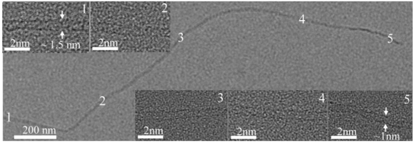
LANE achieved facial synthesis diameter–modulated CNTs by controlling substrate temperatures instantly through tuning the incident laser power [63]. Single–walled CNTs with increasing diameters were grown by reducing the growth temperature from 650 to 450 oC, as shown in (Figure 14). In Raman spectra of the vertically aligned single–walled CNTs, both low and high frequency RBM peaks were observed at the starting end of the CNT, while only low frequency RBM peak was observed at the other end, indicating the increase in tube diameters from one end to the other.
Figure 14: A TEM micrograph of a single-walled CNT grown with a descending temperature profile from 650 to 450 oC. The zoomed views, (1 - 5), corresponding to the labeled areas of the tube, show the tube diameter changes from one end to the other.
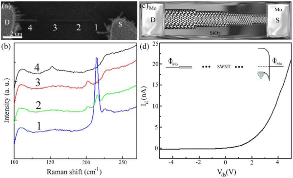
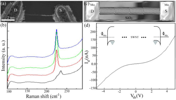
I–V characteristics and Raman spectra of CNT–FETs fabricated with a diameter–modulated and a regular single–walled CNT are compared and shown in (Figure 15 and 16). The device with the diameter–modulated single–walled CNT exhibits a diode–like I–V curve, Figure 15, whereas the device with the uniform one has an almost symmetrical I–V curve, (Figure 16). The device with the diameter–modulated single–walled CNT forms two different contacts with the metallic electrodes. One side forms a Schottky barrier between the Mo electrode and the single–walled CNT end with the smaller diameter (a larger band gap). The other side formsan Ohmic contact between the Mo electrode and the single–walled CNT end with the larger diameter (a smaller band gap). The band diagram of the device is shown in the inset of (Figure 15d). When the device was positively biased (Vds > 0) and the Schottky contact (source) was grounded, positive current value was obtained. When negatively biased (Vds < 0), no current flew through the device. Based on the previous studies, single–walled CNTs can form either Schottky barriers or Ohmic contacts with different metals, depending on the work function of the metal to contact with. Using a uniform single–walled CNT, forming a diode by contacting the tube with two different metals would increase the fabrication complexity, time, and cost [118–120]. Using a diameter–modulated single–walled CNT, different band gaps at the two ends of the tube can form a diode by simply bridging the single–walled CNT with two electrodes of the same metal. This approach significantly simplifies the processes to fabricate CNT–based Schottky diodes. Micro–Raman spectroscopy of the single–walled CNTs was conducted by mapping the tubes with 1 μm steps to investigate the diameter modulation and corresponding band gap changing along the tubes as assigned in the Kataura plot [121]. As shown in (Figure 15), the RBM peak frequency is much higher on one side (grown under higher temperature) and shifts to a lower frequency on the other side (grown under lower temperature) of the single–walled CNT. The double–peak feature obtained at position2 indicates an inter–junction area since the higher peak is the same as that of position 1 and lower peak is the same as that of position 3 of the tube. At the same time, it was observed that the electrical currents were much smaller in diameter–modulated single–walled CNTs than regular tubes, due to the electron scattering caused by the defects.
Figure 15: (a) SEM image of a single-walled CNT bridging Mo electrodes. (b) Raman spectra at different locations on the tube shown in (a). (c) The schematic representation of the tube structure. (d) The typical I-V characteristics showing a diodelike behavior of the device with an inset indicating the expected band diagram.
Figure 16: (a) SEM image of a single-walled CNT bridging the Mo electrodes. (b) The corresponding Raman spectra. (c) The schematic representation of the structure. (d) I-V characteristics showing almost symmetrical conductance in both directions with an inset indicating the expected band diagram.
Fabricating Plasmonic–Enhanced CNT Infrared Bolometers
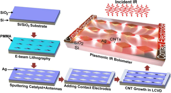
Based on the laser–assisted CNT growth and integration techniques, LANE successfully fabricated plasmonic–enhanced CNT infrared (IR) bolometers by integrating CNTs into metallic nanoantenna arrays, [62] as illustrated in (Figure 17). Due to the strong localized optical field in the gaps of the nanoantenna arrays, a responsively of 800 V⁄W was achieved at room temperature [62].
Figure 17: Schematic flowchart showing the fabrication process for the IR bolometers with CNT-integrated nanoantenna arrays.
Laser–Assisted Fabrication of Zero–Dimensional Carbon Nanoonions
Carbon nano–onions (CNOs) are concentric multilayer giant fullerenes, which consist of multiple concentric graphitic shells to form encapsulated structures [122]. As an important member in the fullerene family, CNOs have been investigated extensively to replace fullerenes due to their extreme similarities shared with fullerenes but at a much lower cost [4, 123–128]. A wide spectrum of applications have been envisioned for CNOs, including gas storage, super capacitors, broadband electromagnetic shielding, catalyst support structures, nanolubricating additives, and water purification [4, 123– 133]. Therefore, scalable production of quality CNOs is desired.
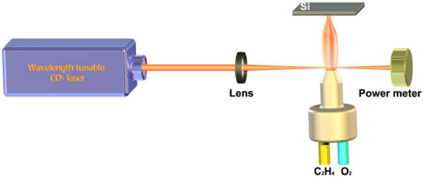
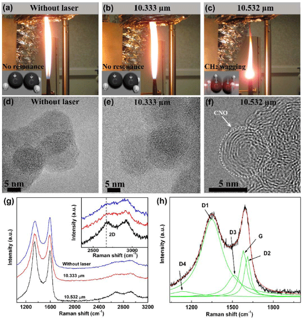
In LANE, a laser–assisted combustion method, (Figure 18), was developed to achieve catalyst–free and scalable growth of CNOs in open air by using laser irradiations to achieve resonant excitation of the precursor molecules - ethylene [66]. Both growth rate and crystalline quality of the CNOs were significantly improved by matching the laser irradiation wavelengths with the vibrational states of the ethylene molecules. Highly concentric CNO particles were obtained at a laser wavelength of 10.532 μm, which resonantly excited the CH2 wagging mode (ν7, 949.3 cm– 1) of the ethylene molecules. A growth rate up to 2.1 g h–1 was recorded, which is higher than that of without laser (1.3 g h–1).
Figure 18: Schematic experimental setup of the laser-assisted combustion system.
The ethylene–oxygen flame becomes obviously brighter and shorter (Figure 19c) when resonantly excited (10.532 μm) compared with the cases without laser excitation (Figure 19a) and a nonresonant excitation at 10.333 μm (Figure 19b). CNOs produced under the resonant excitation conditions (10.532 μm) demonstrate obviously improved crystallinity showing concentric structures containing long–range ordered graphitic striations. (Figure 19g) shows typical Raman spectra of the CNOs. The inset shows a zoomed view of the second–order Raman peaks. In the Raman spectra, the Dand G–bands are observed at 1350 and 1590 cm–1, respectively, and fitted into five different bands (G, D1, D2, D3, and D4), [134, 135] as shown in (Figure. 19h) Herein, the full width at half maximum (FWHM) of the G–bands and the relative intensities (R3= ID3⁄(ID3 + ID2 +IG)) of the D3 bands were analyzed [134, 135]. By comparing the CNOs grown under different circumstances, the decreased G–band FWHM, reduced R3 ratio, and increased 2D–band ((˜ 2690 cm–1) intensity indicates the improvement in the crystallinity of theCNOs grown with the resonant excitation at 10.532 μm. The CNO growth rate at 10.532 μm was measured to be around 2.1 g h–1, which was higher than that at 10.333 μm (0.3 g h–1) and without laser (1.3 g h– 1). Therefore, the resonant excitation of the C2H4 molecules at 10.532 μm not only improves the crystallinity of CNOs but also increases the growth rate.
Figure 19: Photographs of ethylene-oxygen flames: (a) without laser excitation, (b) excited at 10.333 μm, and (c) excited at 10.532 μm (The insets show molecular vibration under the excitation conditions). TEM images of CNOs grown (d) without laser excitation and with laser excitations at (e) 10.333 and (f) 10.532 μm. (g) Raman spectra of CNOs grown without laser excitation and with laser excitations at 10.333 and 10.532 μm (The inset shows the magnified view of the second-order Raman spectra). (h) Typical curve fitting of a firstorder Raman spectrum.
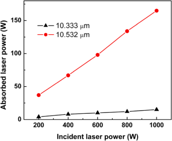
To study the influence of laser–induced resonant excitation of ethylene molecules on the CNO growth, laser absorption by the flame at the non–resonant wavelength of 10.333 μm and the resonant wavelength of 10.532 μm was investigated, as shown in (Figure 20). A much stronger absorption was observed at the wavelength of 10.532 μm, and ascribed to the resonant excitation of the CH2 wagging mode (ν7, 949.3 cm–1) of the C2H4 molecules. By absorbing laser energy at 10.532 μm, the CH2 wagging mode is resonantly excited. In this approach, laser energy was coupled into the flame more efficiently. The total absorbed laser power is much higher at an excitation laser wavelength of 10.532 μm than a non–resonant one, such as 10.333 μm, as shown in ( 20). At the laser wavelength of 10.532 μm, starting from the threshold laser power of 400 W, sufficiently high temperature in the flame is reached by the efficient coupling of the laser energy through resonant excitation to decompose polycyclic aromatic hydrocarbons (PAHs) into C2 species, which favor the formation of more ordered graphitic layers [136]. Hence, CNOs with long–range ordered concentric graphitic shells are formed.
Figure 20: The laser powers absorbed by the combustion flame at the wavelengths of 10.333 and 10.532 μm as the functions of the incident laser power.
Conclusion
A series of laser–assisted nano–fabrication techniques have been developed in LANE for fabricating various carbon nanostructures and related devices by making use of unique laser material interactions. The unique capabilities of lasers provide irreplaceable approaches addressing grand challenges in the nanostructure fabrication and integration. It is expected that lasers would find more applications in future nanostructure fabrication and device manufacture.
Acknowledgements
The author would like to express his sincere gratitude to his colleagues in the Laser–Assisted Nano Engineering (LANE) laboratory, http:⁄⁄lane.unl.edu, in the Department of Electrical Engineering at the University of Nebraska–Lincoln. Led by Prof. Yong Feng Lu, the LANE carries out vibrant research in laser–related nanoscience and technology aimed at understanding laser–material interactions at the nanoscale and molecular levels and developing application–oriented laser techniques.
The author is also heartily grateful to National Science Foundation (ECCS 0652905, ECCS 0621899, CMMI 0758199, CMMI 0852729, and CMMI 0555884),. Office of Naval Research (MURI N00014–05– 1–0432 and N00014–09–1–0943), Nebraska Research Initiative, and Nebraska Center for Energy Science for their financial support.
References
- Hirsch A. The era of carbon allotropes. Nat Mater. 2010; 9: 868-871.
- Kroto HW, Heath JR, Obrien SC, Curl RF, Smalley RE. C-60 - Buckminsterfullerene. Nature. 1985; 318: 162-163.
- Fabre TS, Treleaven WD, McCarley TD, Newton CL, Landry R, et al. Fullerene-derived carbon allotropes. Synthesis, isolation and characterization of C-122. Abstracts of Papers of the American Chemical Society. 1998; 215: U27-U27.
- Ge A Y, Xu B S, Wang X M, Li T B, Han P D, Liu X G. Study on electromagnetic property of nano onion-like fullerenes. Acta Physico-Chimica Sinica. 2006; 22: 203-208.
- Komatsu K, Fujiwara K, Tanaka T, Murata Y. The fullerene dimer C-120 and related carbon allotropes. Carbon. 2000; 38: 1529-1534.
- Kroto H W. Carbon Allotropes - Carbon Onions Introduce New Flavor to Fullerene Studies. Nature. 1992: 359: 670-671.
- Iijima S. Helical Microtubules of Graphitic Carbon. Nature. 1991; 354: 56-58.
- Novoselov K S, Geim A K, Morozov S V, Jiang D, Zhang Y, Dubonos S V, et al. Electric field effect in atomically thin carbon films. Science. 2004; 306: 666-669.
- Novoselov KS1, Jiang D, Schedin F, Booth TJ, Khotkevich VV, Morozov SV, et al. Two-dimensional atomic crystals. Proc Natl Acad Sci U S A. 2005; 102: 10451-10453.
- Collins PG, Avouris P. Nanotubes for electronics. Sci Am. 2000; 283: 62-69.
- Appenzeller J, Knoch J, Martel R, Derycke V, Wind S J, Avouris P. Carbon nanotube electronics. Ieee Transactions on Nanotechnology. 2002; 1: 184-189.
- Appenzeller J, Martel R, Derycke V, Radosavjevic M, Wind S, Neumayer D, et al. Carbon nanotubes as potential building blocks for future nanoelectronics. Microelectronic Engineering. 2002; 64: 391-397.
- Avouris P, Chen J. Nanotube electronics and optoelectronics. Materials Today. 2006; 9: 46-54.
- Avouris P, Chen J, Freitag M, Perebeinos V, Tsang J C. Carbon nanotube optoelectronics. Physica Status Solidi B-Basic Solid State Physics. 2006; 243: 3197-3203.
- Avouris P1, Chen Z, Perebeinos V. Carbon-based electronics. Nat Nanotechnol. 2007; 2: 605-615.
- Avouris P, Martel R, Derycke V, Appenzeller J. Carbon nanotube transistors and logic circuits. Physica B-Condensed Matter. 2002; 323: 6-14.
- Bachtold A1, Hadley P, Nakanishi T, Dekker C. Logic circuits with carbon nanotube transistors. Science. 2001; 294: 1317-1320.
- Bachtold A, Hadley P, Nakanishi T, Dekker C. Logic circuits based on carbon nanotubes. Physica E-Low-Dimensional Systems & Nanostructures. 2003; 16: 42-46.
- Baughman RH1, Zakhidov AA, de Heer WA. Carbon nanotubes--the route toward applications. Science. 2002; 297: 787-792.
- Bonaccorso F, Sun Z, Hasan T, Ferrari A C. Graphene photonics and optoelectronics. Nature Photonics. 2010; 4: 611-622.
- Dai H J. Carbon nanotube as a model system for nanoscale science. Abstracts of Papers of the American Chemical Society. 2002; 223: C46-C46.
- Dai H J. Carbon nanotubesμ opportunities and challenges. Surface Science. 2002; 500: 218-241.
- Geim AK1, Novoselov KS. The rise of graphene. Nat Mater. 2007; 6: 183-191.
- Hoenlein W, Kreupl F, Duesberg G S, Graham A P, Liebau M, Seidel R V, et al. Carbon nanotube applications in microelectronics. Ieee Transactions on Components and Packaging Technologies. 2004; 27: 629-634.
- Soldano C, Mahmood A, Dujardin E. Production, properties and potential of graphene. Carbon. 2010; 48: 2127-2150.
- Blake P1, Brimicombe PD, Nair RR, Booth TJ, Jiang D, Schedin F, et al. Graphene-based liquid crystal device. Nano Lett. 2008; 8: 1704-1708.
- Hecht DS1, Hu L, Irvin G. Emerging transparent electrodes based on thin films of carbon nanotubes, graphene, and metallic nanostructures. Adv Mater. 2011; 23: 1482-1513.
- Hu Y H, Shenderova O A, Hu Z, Padgett C W, Brenner D W. Carbon nanostructures for advanced composites. Reports on Progress in Physics. 2006; 69: 1847-1895.
- Kaushik B K, Goel S, Rauthan G. Future VLSI interconnectsμ optical fiber or carbon nanotube - a review. Microelectronics International. 2007: 24: 53-63.
- Kim KS1, Zhao Y, Jang H, Lee SY, Kim JM, Kim KS, et al. Large-scale pattern growth of graphene films for stretchable transparent electrodes. Nature. 2009; 457: 706-710.
- Kim Y K, Park H. Light-harvesting carbon allotropes platforms for photocatalytic hydrogen production from water. Abstracts of Papers of the American Chemical Society. 2011; 242.
- Kreupl F, Graham A P, Duesberg G S, Steinhogl W, Liebau M, Unger E, et al. Carbon nanotubes in interconnect applications. Microelectronic Engineering. 2002; 64: 399-408.
- Martel R, Derycke V, Appenzeller J, Wong PHS, Avouris P. Carbon nanotube field-effect transistors and logic devices. Abstracts of Papers of the American Chemical Society. 2001; 222: U184-U185.
- Martel R, Schmidt T, Shea H R, Hertel T, Avouris P. Single- and multi-wall carbon nanotube field-effect transistors. Applied Physics Letters. 1998; 73: 2447-244.
- Prasher R. Graphene Spreads the Heat. Science. 2010; 328: 185-186.
- rasher R. Materials science. Graphene spreads the heat. Science. 2010; 328: 185-186.
- Wassei J K, Kaner R B. Graphene, a promising transparent conductor. Materials Today. 2010; 13: 52-59.
- Yousif MY1, Lundgren P, Ghavanini F, Enoksson P, Bengtsson S. CMOS considerations in nanoelectromechanical carbon nanotube-based switches. Nanotechnology. 2008; 19: 285204.
- vouris P. Molecular electronics with carbon nanotubes. Acc Chem Res. 2002; 35: 1026-1034.
- Avouris P. Carbon nanotube electronics. Chemical Physics. 2002; 281: 429-445.
- Avouris P. Nanotube electronics - Electronics with carbon nanotubes. Physics World. 2007; 20: 40-45.
- Hayashi T1, Kim YA, Natsuki T, Endo M. Mechanical properties of carbon nanomaterials. Chemphyschem. 2007; 8: 999-1004.
- Freitag M, Martin Y, Misewich J A, Martel R, Avouris P H. Photoconductivity of single carbon nanotubes. Nano Letters. 2003; 3: 1067-1071.
- Kong J1, Franklin NR, Zhou C, Chapline MG, Peng S, Cho K, et al. Nanotube molecular wires as chemical sensors Science. 2000; 287: 622-625.
- Liang X L, Wang S, Wei X L, Ding L, Zhu Y Z, et al. Towards Entire-Carbon-Nanotube Circuitsμ The Fabrication of Single-Walled-Carbon- Nanotube Field-Effect Transistors with Local Multiwalled-Carbon-Nanotube Interconnects. Advanced Materials. 2009; 21: 1339-1343.
- Sharma P, Ahuja P. Recent advances in carbon nanotube-based electronics. Materials Research Bulletin. 2008? 43μ 2517-2526.
- Yang SB1, Kong BS, Jung DH, Baek YK, Han CS, Oh SK, et al. Recent advances in hybrids of carbon nanotube network films and nanomaterials for their potential applications as transparent conducting films. Nanoscale. 2011; 3: 1361-1373.
- Kabashin A1, Delaporte P, Pereira A, Grojo D, Torres R, Sarnet T, et al. Nanofabrication with pulsed lasers. Nanoscale Res Lett. 2010; 5: 454-463.
- Majumdar J D, Manna I. Laser material processing. International Materials Reviews. 2011; 56: 341-388.
- Cheng DD, Yu RQ, Liu ZY, Zhang Q, Wang YH, et al. Preparation of Carbon Nanotubes from Laser-Ablation. Chemical Journal of Chinese Universities-Chinese. 1995; 16: 948-949.
- Wang YH, Zhang QA, Liu ZY, Huang RB, Zheng LS. Production of Carbon Nanotubes at Carbon/Water Interface by Pulsed-Laser Ablation. Acta Physico-Chimica Sinica. 1996; 12: 905-909.
- Juha L, Ehrenberg B, Couris S, Koudoumas E, Hamplova V, et al. Fullerene decomposition induced by near-infrared laser radiation studied by real-time turbidimetry. Chemical Physics Letters. 1999; 313: 431-436.
- Tang ZC, Huang RB, Chen H, Zheng LS. Laser productions of fullerene ions promoted by additive compounds in carbon targets. Journal of Physical Chemistry A. 1998; 102: 9993- 9998.
- Laska L, Krasa J, Juha L, Hamplova V, Soukup L. Fullerene production driven by long- pulses of near-infrared laser radiation. Carbon. 1996; 34: 363-368.
- Xie ZX, Liu ZY, Wang CR, Huang RB, Lin FC, et al. Formation and Coalescence of Fullerene Ions from Direct Laser Vaporization. Journal of the Chemical Society- Faraday Transactions. 1995; 91: 987-990.
- Huang RB, Huang F, Liu ZY, Wang CR, Lin FC, et al. Aggregations of Fullerene Anions in Laser Plasma. Acta Physico-Chimica Sinica. 1994; 10: 925-927.
- Park JB, Xiong W, Gao Y, Qian M, Xie ZQ, et al. Fast growth of graphene patterns by laser direct writing. Applied Physics Letters. 2011; 98: 123109.
- Park JB, Xiong W, Xie ZQ, Gao Y, Qian M, et al. Transparent interconnections formed by rapid single-step fabrication of graphene patterns. Applied Physics Letters. 2011; 99: 053103.
- Qian M, Zhou YS, Gao Y, Feng T, Sun Z, et al. Production of few-layer graphene through liquid-phase pulsed laser exfoliation of highly ordered pyrolytic graphite. Applied Surface Science. 2012; 258: 9092-9095.
- Qian M, Zhou YS, Gao Y, Park JB, Feng T, et al. Formation of graphene sheets through laser exfoliation of highly ordered pyrolytic graphite. 2011; 98: 173108.
- Applied Physics Letters. 2011; 98:
- Zhou YS, Xiong W, Gao Y, Mahjouri-Samani M, Mitchell M, et al. Towards carbon-nanotube integrated devicesμ optically controlled parallel integration of single-walled carbon nanotubes. Nanotechnology. 2010; 21: 315601.
- Xiong W1, Zhou YS, Mahjouri-Samani M, Yang WQ, Yi KJ, He XN, et al. Self-aligned growth of single-walled carbon nanotubes using optical near-field effects. Nanotechnology. 2009; 20: 025601.
- Mahjouri-Samani M1, Zhou YS, He XN, Xiong W, Hilger P, Lu YF. Plasmonic-enhanced carbon nanotube infrared bolometers. Nanotechnology. 2013; 24: 035502.
- Mahjouri-Samani M, Zhou YS, Xiong W, Gao Y, Mitchell M, et al. Diameter modulation by fast temperature control in laser-assisted chemical vapor deposition of single- walled carbon nanotubes. Nanotechnology. 2010; 21: 395601.
- Mahjouri-Samani M1, Zhou YS, Xiong W, Gao Y, Mitchell M, Lu YF. Laser induced selective removal of metallic carbon nanotubes. Nanotechnology. 2009; 20: 495202.
- Gao Y, Zhou YS, Xiong W, Mahjouri-Samani M, Mitchell M, et al. Controlled growth of carbon nanotubes on electrodes under different bias polarity. Applied Physics Letters. 2009; 95: 143117
- Gao Y, Zhou YS, Park JB, Wang H, He XN, et al. Resonant excitation of precursor molecules in improving the particle crystallinity, growth rate and optical limiting performance of carbon nano-onions. Nanotechnology. 2011; 22: 165604.
- Bunch JS1, Verbridge SS, Alden JS, van der Zande AM, Parpia JM, Craighead HG, et al. Impermeable atomic membranes from graphene sheets. Nano Lett. 2008; 8: 2458-2462.
- Lee C1, Wei X, Kysar JW, Hone J. Measurement of the elastic properties and intrinsic strength of monolayer graphene. Science. 2008; 321: 385-388.
- Aristov VY1, Urbanik G, Kummer K, Vyalikh DV, Molodtsova OV, Preobrajenski AB, et al. Graphene synthesis on cubic SiC/Si wafers. perspectives for mass production of graphene-based electronic devices. Nano Lett. 2010; 10: 992-995.
- utter P. Epitaxial graphene: How silicon leaves the scene. Nat Mater. 2009; 8: 171-172.
- Bae S1, Kim H, Lee Y, Xu X, Park JS, Zheng Y, et al. Roll-to-roll production of 30-inch graphene films for transparent electrodes. Nat Nanotechnol. 2010; 5: 574-578.
- Lee Y1, Bae S, Jang H, Jang S, Zhu SE, Sim SH, et al. Wafer-scale synthesis and transfer of graphene films. Nano Lett. 2010; 10: 490-493.
- Li X1, Cai W, An J, Kim S, Nah J, Yang D, et al. Large-area synthesis of high-quality and uniform graphene films on copper foils. Science. 2009; 324: 1312-1314.
- Sun Z1, Yan Z, Yao J, Beitler E, Zhu Y, Tour JM. Growth of graphene from solid carbon sources. Nature. 2010; 468: 549-552.
- Becerril HA, Stoltenberg RM, Tang ML, Roberts ME, Liu ZF, et al. Fabrication and Evaluation of Solution-Processed Reduced Graphene Oxide Electrodes for p- and n-Channel Bottom-Contact Organic Thin-Film Transistors. Acs Nano. 2010; 4: 6343-6352.
- He Q1, Sudibya HG, Yin Z, Wu S, Li H, Boey F, et al. Centimeter-long and large-scale micropatterns of reduced graphene oxide films: fabrication and sensing applications. ACS Nano. 2010; 4: 3201-3208.
- Joung D, Chunder A, Zhai L, Khondaker S I. High yield fabrication of chemically reduced graphene oxide field effect transistors by dielectrophoresis. Journal of Nanoscience and Nanotechnology. 2010; 21: 1239-1267. Mostofizadeh A, Li YW, Song B, Huang YD. Synthesis, Properties, and Applications of Low-Dimensional Carbon-Related Nanomaterials. Journal of Nanomaterials. 2011; 2011: 685081.
- Ghosh S1, Sood AK, Kumar N. Carbon nanotube flow sensors. Science. 2003; 299: 1042-1044.
- Javey A1, Guo J, Wang Q, Lundstrom M, Dai H. Ballistic carbon nanotube field-effect transistors. Nature. 2003; 424: 654-657.
- Javey A1, Kim H, Brink M, Wang Q, Ural A, Guo J, et al. High-kappa dielectrics for advanced carbon-nanotube transistors and logic gates. Nat Mater. 2002; 1: 241-246.
- Li H, Xu C, Srivastava N, Banerjee K. Carbon Nanomaterials for Next-Generation Interconnects and Passives & Physics, Status, and Prospects. Ieee Transactions on Electron Devices. 2009; 56: 1799-1821.
- Martel R1, Derycke V, Lavoie C, Appenzeller J, Chan KK, Tersoff J, et al. Ambipolar electrical transport in semiconducting single-wall carbon nanotubes. Phys Rev Lett. 2001; 87: 256805.
- Derycke V, Martel R, Appenzeller J, Avouris P. Carbon nanotube inter- and intramolecular logic gates. Nano Letters. 2001; 1: 453-456.
- LeMieux MC1, Roberts M, Barman S, Jin YW, Kim JM, Bao Z. Self-sorted, aligned nanotube networks for thin-film transistors. Science. 2008; 321: 101-104.
- Tans SJ, Verschueren ARM, Dekker C. Room-temperature transistor based on a single carbon nanotube. Nature. 1998; 393: 49-52.
- Bobrinetskii II. Methods of Parallel Integration of Carbon Nanotubes during the Formation of Functional Devices for Microelectronics and Sensor Technologies. Russian Microelectronics. 2009; 38: 353-360.
- Falvo MR1, Clary GJ, Taylor RM 2nd, Chi V, Brooks FP Jr, Washburn S, et al. Bending and buckling of carbon nanotubes under large strain. Nature. 1997; 389: 582-584.
- Franklin NR, Wang Q, Tombler TW, Javey A, Shim M, et al. Integration of suspended carbon nanotube arrays into electronic devices and electromechanical systems. Applied Physics Letters. 2002; 81: 13-15.
- Graham AP, Duesberg GS, Hoenlein W, Kreupl F, Liebau M, et al. How do carbon nanotubes fit into the semiconductor roadmap? Applied Physics a-Materials Science & Processing. 2005; 80: 1141- 1151.
- Graham AP, Duesberg GS, Seidel R, Liebau M, Unger E, et al. Towards the integration of carbon nanotubes in microelectronics. Diamond and Related Materials. 2004; 13: 1296-1300.
- Tseng YC, Xuan PQ, Javey A, Malloy R, Wang Q, et al. Monolithic integration of carbon nanotube devices with silicon MOS technology. Nano Letters. 2003; 4: 123-127.
- Wei YY, Eres G. Directed assembly of carbon nanotube electronic circuits. Applied Physics Letters. 2000; 76: 3759-3761.
- Wei YY, Eres G. Direct fabrication of carbon nanotube circuits by selective area chemical vapour deposition on pre-patterned structures. Nanotechnology. 2000; 11: 61-64.
- Wei YY, Fan X, Eres G. Directed assembly of carbon nanotube electronic circuits by selective area chemical vapor deposition on prepatterned catalyst electrode structures. Journal of Vacuum Science & Technology B. 2000; 18: 3586-3589.
- Duan X1, Zhang J, Ling X, Liu Z. Nano-welding by scanning probe microscope. J Am Chem Soc. 2005; 127: 8268-8269.
- Lefebvre J, Lynch JF, Llaguno M, Radosavljevic M, Johnson AT. Single-wall carbon nanotube circuits assembled with an atomic force microscope. Applied Physics Letters. 1999; 75: 3014-3016.
- Keren K1, Berman RS, Buchstab E, Sivan U, Braun E. DNA-templated carbon nanotube field-effect transistor. Science. 2003; 302: 1380-1382.
- Nagahara LA, Amlani I, Lewenstein J, Tsui RK. Directed placement of suspended carbon nanotubes for nanometer-scale assembly. Applied Physics Letters. 2002; 80: 3826-3828.
- Xin H1, Woolley AT. DNA-templated nanotube localization. J Am Chem Soc. 2003; 125: 8710-8711.
- Chan R H M, Fung C K M, Li W J. Rapid assembly of carbon nanotubes for nanosensing by dielectrophoretic force. Nanotechnology. 2004; 15: S672-S677.
- Chung J, Lee KH, Lee J, Ruoff RS. Toward large-scale integration of carbon nanotubes. Langmuir. 2004; 20: 3011-3017.
- Fung CKM, Wong VTS, Chan RHM, Li WJ. Dielectrophoretic batch fabrication of bundled carbon nanotube thermal sensors. Ieee Transactions on Nanotechnology. 2004; 3: 395-403.
- Li J Q, Zhang Q, Peng N, Zhu Q. Manipulation of carbon nanotubes using AC dielectrophoresis. Applied Physics Letters. 2005; 86: 153116.
- Dresselhaus MS, Dresselhaus G, Saito R, Jorio A. Raman spectroscopy of carbon nanotubes. Physics Reports-Review Section of Physics Letters. 2005; 40: 47-99.
- Jorio A, Saito R, Hafner J H, Lieber C M, Hunter M, et al. Structural (n, m) determination of isolated single-wall carbon nanotubes by resonant Raman scattering. Physical Review Letters. 2001; 86: 1118-1121.
- Souza AG, Chou SG, Samsonidze GG, Dresselhaus G, Dresselhaus MS, et al. Stokes and anti-Stokes Raman spectra of small-diameter isolated carbon nanotubes. Physical Review B. 2004; 69: 115428.
- Hayazawa N, Yano T, Watanabe H, Inouye Y, Kawata S. Detection of an individual single-wall carbon nanotube by tip-enhanced near-field Raman spectroscopy. Chemical Physics Letters. 2003; 376: 174-180.
- Novotny L, Bian R X, Xie X S. Theory of nanometric optical tweezers. Physical Review Letters. 1997; 79: 645-648.
- Brown S D M, Jorio A, Corio P, Dresselhaus M S, Dresselhaus G, et al. Origin of the Breit-Wigner-Fano lineshape of the tangential G-band feature of metallic carbon nanotubes. Physical Review B. 2001; 63: 155414.
- Jorio A, Souza A G, Dresselhaus G, Dresselhaus M S, Swan A K, et al. G-band resonant Raman study of 62 isolated single-wall carbon nanotubes. Physical Review B. 2002; 65: 155412.
- Saito R, Jorio A, Hafner J H, Lieber C M, Hunter M, et al. Chirality-dependent G-band Raman intensity of carbon nanotubes. Physical Review B. 2001; 64: 085312.
- Miyata Y, Yanagi K, Maniwa Y, Kataura H. Optical properties of metallic and semiconducting single-wall carbon nanotubes. Physica Status Solidi B-Basic Solid State Physics. 2008; 245: 2233-2238.
- Wildoer J W G, Venema L C, Rinzler A G, Smalley R E, Dekker C. Electronic structure of atomically resolved carbon nanotubes. Nature. 1998; 391: 59-62.
- Yao Y G, Dai X C, Liu R, Zhang J, Liu Z F. Tuning the Diameter of Single-Walled Carbon Nanotubes by Temperature-Mediated Chemical Vapor Deposition. Journal of Physical Chemistry C. 2009; 113: 13051-13059.
- Yao Y1, Li Q, Zhang J, Liu R, Jiao L, Zhu YT, et al. Temperature-mediated growth of single-walled carbon-nanotube intramolecular junctions. Nat Mater. 2007; 6: 283-286.
- Lu C G, An L, Fu Q A, Liu J, Zhang H, et al. Schottky diodes from asymmetric metal-nanotube contacts. Applied Physics Letters. 2006; 88: 133501.
- Manohara HM1, Wong EW, Schlecht E, Hunt BD, Siegel PH. Carbon nanotube Schottky diodes using Ti-Schottky and Pt-Ohmic contacts for high frequency applications. Nano Lett. 2005; 5: 1469-1474.
- Yang M H, Teo K B K, Milne W I, Hasko D G. Carbon nanotube Schottky diode and directionally dependent field-effect transistor using asymmetrical contacts. Applied Physics Letters. 2005; 87: 253116.
- Kataura H, Kumazawa Y, Maniwa Y, Umezu I, Suzuki S, et al. Optical properties of single-wall carbon nanotubes. Synthetic Metals. 1999; 103: 2555-2558.
- garte D. Curling and closure of graphitic networks under electron-beam irradiation. Nature. 1992; 359: 707-709.
- Chhowalla M1, Wang H, Sano N, Teo KB, Lee SB, Amaratunga GA. Carbon onions: carriers of the 217.5 nm interstellar absorption feature. Phys Rev Lett. 2003; 90: 155504.
- Henrard L, Malengreau F, Rudolf P, Hevesi K, Caudano R, et al. Electron-energy-loss spectroscopy of plasmon excitations in concentric-shell fullerenes. Physical Review B. 1999; 59: 5832-5836.
- Hou S M, Tao C G, Zhang G M, Zhao X Y, Xue Z Q, et al. Ultrahigh vacuum scanning probe microscopy studies of carbon onions. Physica E. 2001; 9: 300-304.
- Lee G H, Huh S H, Jeong J W, Ri H C. Excellent magnetic properties of fullerene encapsulated ferromagnetic nanoclusters. Journal of Magnetism and Magnetic Materials. 2002; 246: 404-411.
- Pichler T, Knupfer M, Golden M S, Fink J, Cabioc'h T. Electronic structure and optical properties of concentric-shell fullerenes from electron-energy-loss spectroscopy in transmission. Physical Review B. 2001; 63: 155415.
- Xu B S. Prospects and research progress in nano onion-like fullerenes. New Carbon Materials. 2008; 23: 289-301.
- Maksimenko S A, Rodionova V N, Slepyan G Y, Karpovich V A, Shenderova O, et al. Attenuation of electromagnetic waves in onion-like carbon composites. Diamond and Related Materials. 2007; 16: 1231-1235.
- Portet C, Yushin G, Gogotsi Y. Electrochemical performance of carbon onions, nanodiamonds, carbon black and multiwalled nanotubes in electrical double layer capacitors. Carbon. 2007; 45: 2511-2518.
- Sano N, Wang H, Alexandrou I, Chhowalla M, Teo K B K, Amaratunga G A J, Iimura K. Properties of carbon onions produced by an arc discharge in water. Journal of Applied Physics. 2002; 92: 2783-2788.
- Yang X W, Guo J J, Wang X M, Liu X G, Xu B S. Study on characterization and growth mechanism of Pt/onion-like fullerenes catalyst. Acta Physico-Chimica Sinica. 2006; 22: 967-971.
- Yao Y L, Wang X M, Guo J J, Yang X W, Xu B S. Tribological property of onion-like fullerenes as lubricant additive. Materials Letters. 2008; 62: 2524-2527.
- Knauer M, Carrara M, Rothe D, Niessner R, Ivleva N P. Changes in Structure and Reactivity of Soot during Oxidation and Gasification by Oxygen, Studied by Micro-Raman Spectroscopy and Temperature Programmed Oxidation. Aerosol Science and Technology. 2008; 43: 1-8.
- Sadezky A, Muckenhuber H, Grothe H, Niessner R, Poschl U. Raman micro spectroscopy of soot and related carbonaceous materials. Spectral analysis and structural information. Carbon. 2005; 43: 1731-1742.
- Vander Wal RL, Tomasek A J. Soot nanostructure and dependence upon synthesis conditions. Combustion and Flame. 2004; 136: 129-140.
