
Special Article on Packing and Reliability of Nano and Micro-electro-mechanical-system (N/MEMS) Devices
Austin J Nanomed Nanotechnol. 2014;2(6): 1032.
Overcoming Some of the Challenges in 3D Micro-Assembly Techniques to Package MEMS Devices
Rezaeisaray M, Lueke J, El Gowini M, Yue S, Raboud D and Moussa W*
Department of Mechanical Engineering, University of Alberta, Canada
*Corresponding author: Moussa W, Department of Mechanical Engineering, University of Alberta, Canada
Received: July 25, 2014; Accepted: August 20, 2014; Published: August 22, 2014
Abstract
This article compiles the most important packaging techniques for micro electromechanical systems (MEMS). In addition, the main electrical interconnection techniques are investigated: wire-bonding, tape automated bonding (TAB), adhesive-based bonding, and flip-chipping. For each specific technique, some examples are demonstrated which were developed or adapted in our lab. A low cost micro-dispensing technique has been developed to run precise dispensing using manual dispensers. An improvised approach of using flexible printed circuit boards (PCBs) as well as conventional solid PCBs is depicted to electrically bond MEMS prototypes and prepare for tests. This article demonstrates adapting 3D printing for packaging of overhanging MEMS structures. This packaging technique is known for its low cost and quick manufacturing capacity and it is also capable of building structures with bio-compatible materials. Additionally, a small vacuum chamber has been designed and manufactured to examine the mechanical response of MEMS devices under vacuum before fully package them. Although this paper provides a platform to deal with some of the main 3D packaging challenges, the same techniques could be expanded for numerous applications and for mass production of MEMS devices.
Keywords: Packaging; Micro-assembly; Wire-bonding; TAB; Flip-chipping; Adhesives
Introduction
The packaging is a vital bridge between semiconductors and printed circuit boards (PCBs) [1]. Packaging in general terms is categorized in various subsections such as biological micro-electromechanical systems (bio MEMS) packaging [2,3], packaging of optoelectronics [4] and radio frequency (RF) devices package [5]. However, the package must satisfy multiple functions including: protection (from the surrounding environment); connectivity (electrical, material transport, radiant energy, external force); compatibility (chip-to-package, package to PCB); routing (electrical, materials); mechanical stress control; thermal management; assembly simplification; testability; and rework ability [1]. Although the packaging, testing and calibration importance and cost (70% of the manufacturing cost [6]) are more than even fabrication, it has gained less consideration in literature. It is known that the packaging belongs to industrial and commercial fields [7]. However in this article, the focus is on low cost techniques to provide some ideas for MEMS and microelectronics researchers to consider when dealing with their packaging and testing experiences. The article starts with a brief overview of packaging possibilities. Die separation which is the first step of most packaging processes comes next. Then, three possible ways of providing electrical connections are presented followed by two other sections discussing the package for wafer level tests and package for the individual dies.
Available Packaging Techniques for MEMS1
Packaging of micro-sensors and micro-actuators is different than general microelectronic devices [7]. In the case of microelectronics, a particular package type can be used for various chips. The size and number of wire-bonds might change but the shape could be the same. However for MEMS devices, the package design crucially depends on the function of the device [7]. Therefore, the MEMS device and its package must be considered simultaneously to take into account each design's limitations for designing the other.
Individual MEMS devices must be diced and then mounted on a package and attached to a metallic, ceramic or plastic platform. A number of dicing and die-attach [8] techniques have been reported. Wiring and electrical interconnections are usually the next process in packaging. Various packaging techniques have been developed based on the specific device's requirements. Micro fluidic interconnections are needed for micro fluidic devices such as micro pumps and micro valves. Ceramic packaging, which is one of the main techniques of electrical packaging, has been extended to the MEMS packaging. Many commercial micro machined sensors use ceramic packaging. This packaging is expensive comparing to other techniques [9]. However, the high reliability, interesting material properties such as electrical insulation and hermetic sealing and easy shaping keeps ceramic packaging one of the main techniques in electronic packaging. Metal packaging, molded plastic packaging, and multichip modules are some other MEMS packaging methods [10]. Integrated MEMS devices merge microstructures and microelectronics on a single substrate to reduce overall size, electrical noise, and system power requirements. However, there are some challenges in terms of materials, process incompatibilities, and high cost [11-13]. As an alternative, hybrid packaging with separate MEMS device and electronic processes could be exploited [14].
Figure 1 demonstrates the path should be taken in MEMS manufacturing. Table 1 provides a summary of the most important available packaging techniques. Most of the information in Table 1 is taken from [15]. The focus of this article is to investigate electrical interconnections used for MEMS packaging and to review various mechanical packaging techniques developed for individual MEMS devices.
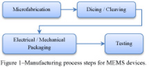
Figure 1: Manufacturing process steps for MEMS devices.
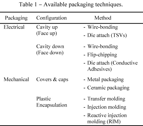
Table 1:
Dicing & Cleaving
Other than the devices to be tested on a wafer level, in most cases the MEMS die has to be separated from the wafer right after fabrication is complete. Dicing is commonly known as a die separation technique. High technology dicing machines provide very thin cutting lines and the blade could be aligned microscopically to cut through the fabricated devices in a short time. A tape is usually used to hold all the separated dies together and prevent them from separating prematurely. Usually a layer of photo resist is spun on the main side of the wafer to protect it from scratches or potential damage due to handling issues. However, in the case of fragile or overhanging (fully released) devices, processing the wafer under dicing machines could easily damage the fabricated devices [2,16]. There has been some research done on improving the reliability of dicing, however, dicing free techniques seemed to be required [17,18]. Laser-based dicing [19] and a diamond scriber [20-22] have also been used to separate dies. In most of the dicing-free attempts, deep reactive ion etching (DRIE) process has widely been used to cleave the silicon substrate [23-29]. Figure 2 demonstrates front and back side of a silicon wafer with numbers of overhanging cantilever designs. The cleaving trenches made by deep backside silicon etching helps to keep the wafer in one piece during handling and at the same time, it provides the capability to easily separate each die from the substrate. This is done by using a modified DRIE process to make two different etch depths on the back side of the silicon wafer [30]. A scanning electron microscope (SEM) picture of two cantilevers after cleaving is shown in Figure 3.
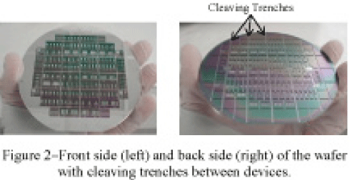
Figure 2: Front side (left) and back side (right) of the wafer with cleaving trenches between devices.
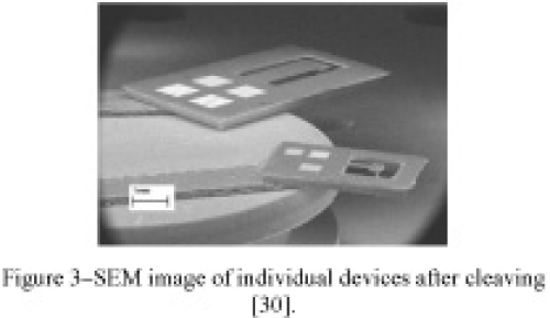
Figure 3: SEM image of individual devices after cleaving [30].
Electrical Interconnection Techniques
Once the devices are diced or cleaved they have to be electrically connected to a printed circuit board (PCB) or other means to apply voltage to the device (in the case of actuators) or receive voltage from the device (in the case of sensors). The standard packaging technologies are: wire bonding, tape automated bonding, dispensing adhesives, flip-chip assembly, soldering, substrate technology and housing technology [4]. Among numbers of techniques to make electrical connections between tiny MEMS devices and a PCB, in this article, three major categories are considered: wire-bonding, tape automated bonding, and flip-chipping. In addition, dispensing adhesives is also presented individually; however, it is usually coupled with flip-chip bonding. Each of these methods has various sub-groups which are briefly introduced in the following sections. The advantages and disadvantages of above techniques are presented in Table 2. Most information for this table is taken from [7,15,31-33].
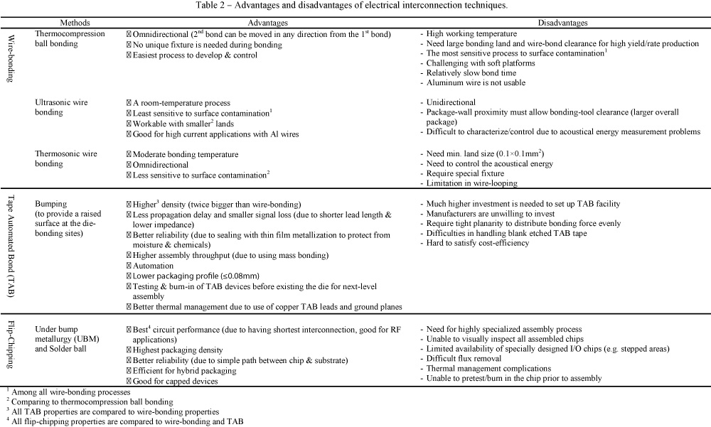
Table 2:
Wire-bonding
Wire-bonding for MEMS is a fairly standard packaging technique. It is known as the most widely used interconnection technique to electrically connect a MEMS die to the package. Typically, gold and aluminum wires are used in wire-bonding but silver and copper wires are also reported [15]. Bonding of gold wire seems to be easier than bonding aluminum wires. However, it is difficult to find gold wires above 50μm diameter, whereas, aluminum wires are available up to 560μm in diameter which makes them the only solution for high current applications [10]. In addition, wire-bonding seems to be problematic for RF applications. The resistance of thin wires and bonds could result in significant losses and, depending on wires' lengths, some parasitic inductance might be added to the system [33]. Soft platforms for the die are a source of challenge for wire-bonding and typically needs coupling of ultrasonic energy into the bonding region [7].
Reliable wire-bonds are essential for proper electrically functionality of the package. In operational point of view, achieving to a proper bond is challenging. Purity and contamination-free wire, optimizing capillary feed, clean operation, and optimized process parameters such as temperature, pressure, and ultrasonic energy must be considered to achieve a reliable bond [15].
In addition to creating wire connections, a wire-bonder may be used for bonding a single ball to a metal pad. Figure 4 demonstrates three different bonds made by West Bond Inc. wire-bonder. A ball-wedge bond is used to connect pads of a chip to pads on a PCB. The single ball, known as a stud bump, is created using a stud bumping tool. The stud bumping process is usually performed in combination with a secondary process, known as coining, which uses a tool with no capillary and a flat tip to compress one or several bumps down to the same height [34]. Coined bumps are used as interconnects in flip chip processes.
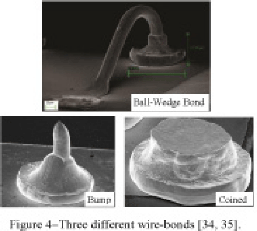
Figure 4: Three different wire-bonds [34,35].
Tape automated bonding
One another integrated circuit die packaging is tape automated bonding (TAB). This fine-pitch packaging technique uses fine-line conductor patterns on a flexible printed circuit or on bare copper [31]. A process called Bumping is used to make raised surfaces at the die bonding region. The bump could be made on the wafer or the tape carrier [31]. TAB is highly costly and some semiconductor manufacturers refuse investing for this technology while they have access to wire-bonding or flip-chipping. However, TAB has some advantages that allow this technology grow over time (Table 2).
Dispensing Adhesives
Adhesives could be used for various purposes such as thermal conduction, electrical conduction, reduce parasitic capacitance between traces and leads, under fill process for flip-chip, and gluing and encapsulating chip on board [32]. In this section, the focus is on dispensing electrically conductive adhesives. Through silicon via (TSV) is a vertical interconnection through the thickness of a silicon substrate enabling electrical conductivity between components on top and bottom of the substrate. A variety of TSV designs has been reported [36-40]. All designs consist of a through hole in the substrate, an insulating layer which prevents current leakage to bulk silicon, metal layers on both sides for the traces or pads, and conductive materials filled in the void. A number of materials have been investigated as conductive fillings such as electroplated copper [41], poly silicon [42,43], conductive adhesive [44,45], tungsten [46], and even wire-bonds to lower the capacitance of the coupling [47]. One another approach was presented using TSVs and flip-chip bonding to package MEMS devices [48]. In this method, conductive epoxy is dispensed into the TSV. Figure 5 demonstrates a 200μm TSV made by cryogenic DRIE in a 500μm thick silicon wafer. Also, cross section and top views of a fully filled TSV are shown. It is challenging to fill high aspect ratio TSVs. Therefore, epoxy is dispensed from both sides of the substrate. This process was performed using a fluid dispensing system with a syringe tip which had an internal diameter of 50μm [48].
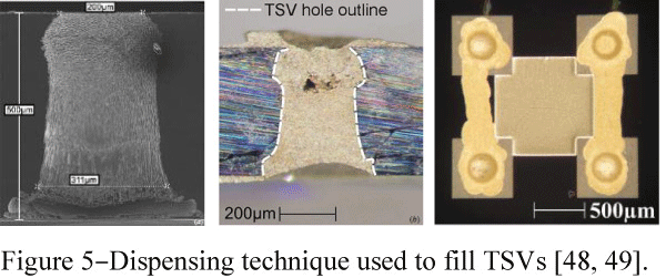
Figure 5: Dispensing technique used to fill TSVs [48,49].
There are a variety of automatic dispensing tools. For instance, Fine tech GmbH & Co. provides submicron die positioning and also offers dispensing of various materials such as optical, thermal, isotropic, and anisotropic conductive adhesives. They also provide rework services for preassembled dies by removing and re-dispensing solder paste. However, automatic dispensing equipment is costly and possibly not available for all researchers to use. Alternatively, manual dispensers are used. The main challenge with manual dispensers is accuracy in positioning due to shaking of the hand. In a new approach, an adapter was designed to hold a dispensing syringe and be installable on a micropositioned which is capable of positioning in three axes within one micrometer accuracy. A micropositioner from Quarter Research and Development (Model XYZ 500 TIS) and a dispensing system from Nordson EFD (Ultimo's II) were used in thiscase. Figure 6 demonstrates the designed adaptor and the orientation of the needle and also presents precisely placed adhesive dots in the middle of tiny pads. The tip of the syringe needs to be oriented in the same orientation as the hole to enhance the filling of a TSV. But, using a straight needle as syringe's tip blocks the microscope view. Therefore, instead of straight needles, angled ones (45O) were used and the 3D printed adaptor was designed such that the syringe was oriented 45° to the surface. Consequently, the tip of the needle is perpendicular to the surface and neither syringe nor the adaptor blocks the user's view.
Figure 6:
Flip-chip bonding
Flip-chip or direct chip attach (DCA) is a low volu e, 3D vertical integration scheme that allows for direct connection between PCB and the die (top-face-down). Capped devices could easily be made by a flip-chipper. DCA provides a number of joining systems from conventional metallic solders to low-temperature conductive polymers. DCA has four subdivisions: device bumps, joining material, and under-fill [1]. There is usually a relatively small gap (50- 200μm) between the die and the packaging substrate [10]. Therefore, the parasitic inductance and capacitance for each interconnection is minimized due to minimum transmission line length which makes the flip-chipping a better packaging technique than wire-bonding for RF applications [33]. In addition, unlike wire-bonding which requires bond pads away from die to prevent wires from crossing, flip-chip involves placing bond pads on top of the die resulting in a significant increase in input/output connection density [10]. Flipchip is attractive for MEMS industry due to providing the capability of packaging a number of dies in a single package substrate with multilevel electrical traces (hybrid packaging). Wire-bonding could also be used to build a similar system, however, not only its area usage will not be as efficient, but also its reliability will be doubtful due to too many wires in the package. One of the disadvantages of flip-chipping is that it is not compatible with released microstructures. For instance, a MEMS device with a thin diaphragm could be damaged during the flip-chip process [10].
Apart from exploiting a flip-chipper to precisely place dies, it can also be used to create electrical and mechanical bonds. Compression-based, thermal-based, ultrasonic-based, or any combination of these methods could be performed to achieve a bond with conductive epoxy, non-conductive epoxy, anisotropic and isotropic films and stud/solder bumps [34]. Figure 7 demonstrates packaging resonators to PCBs with the flip-chip technique. Conductive adhesive dots are placed on the device's pads (using the technique shown in Figure 6) and then the flexible or conventional PCB's pads are flip-chipped on them. Flexible PCBs (FPCBs) are soft and could be cut by scissors. Pads and traces could be designed very close (3μm width, 5μm gap). However, the process is expensive for prototyping. In comparison although solid PCBs are much cheaper, they need a tool to be diced and do not have as high resolution as FPCBs.
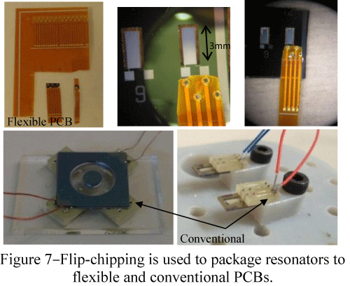
Figure 7:
If the pads on the sensing chip are too close and overflowing is unavoidable, anisotropic conductive adhesive (ACA) could be used to prevent short circuiting of one pad to the ones next to it and also allow vertical electrical connection to the PCB pad on top of it. Figure 8 shows a cross section of a packaged sensing chip on a PCB. In this case, there are many pads and they located close to one another and using ACA seemed to be unavoidable.
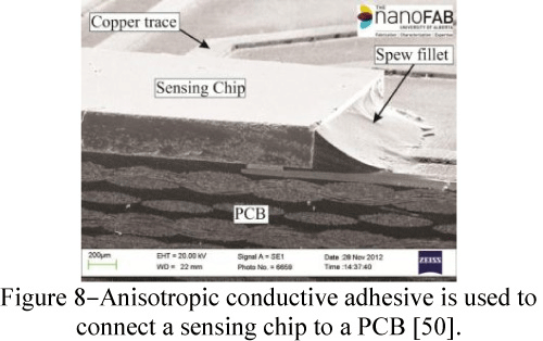
Figure 8:
Figure 9.a demonstrates a top view of a membrane sensor. The design of the sensor requires the face-down packaging configuration. In this case, dispensing adhesive on the pads will overflow on the membrane and affect its performance. Therefore, tall SU-8 layers are deposited to avoid overflowing of the ACA on the membrane. The pads of both sensing chip and the PCB have gold stud bumps and ACA is dispensed on the chip pads and then flip-chipped on the PCB pads (Figure 9.b).
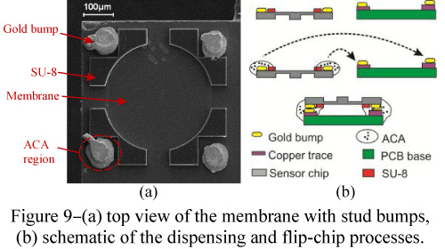
Figure 9:
Packaging for Wafer-Level Tests
Wafer level packaging is usually done for devices made by surface micromachining. This packaging avoids the challenges of separating individual dies and therefore enhances the reliability and yield of the packaging/testing stage. Wafer level packaging is generally done by bonding a lid wafer to the device wafer or by making a cavity through etching a sacrificial layer. Anodic bonding, metal bonding, plasma-activated bonding, and bonding with an intermediate melting material are some of the interfacial bonding techniques used for wafer level packaging [51].
On the other hand, some of the MEMS devices could be tested on the wafer without separating individual dies. A probing station could be exploited to land the probes on the devices' pads. Then, electrical signals could be sent or received from those devices. For instance, in a surface acoustic wave sensor (Figure 100), the input signal is applied through a ground-signal-ground (GSG) probe to the input interdigitated transducer (IDT) and the sensor's response is received by the output IDT. Therefore, the size and location of the pads are the only considerations that need to be taken into account for the packaging during the fabrication masks design.
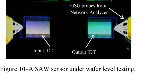
Figure 10:
Package for Individual Devices
As opposed to wafer level testing, sometimes individual MEMS devices have to be separated from the substrate due to testing setup requirements. For instance, to run a bending test on a stress sensor it has to be diced and placed on a bending structure (Figure 11.a). Also, to run a vibration test on a resonator, it must be separated from the substrate and raised from the ground to provide some space for the proof mass to oscillate (Figure 11.b).
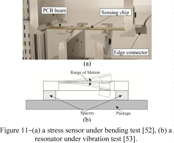
Figure 11:
Therefore, a MEMS device could be directly mounted on a PCB and electrically connected to it using one of above techniques or a mechanical structure is required to optimally mount both device and PCB on it and then electrically connect them. Both methods are demonstrated with examples in the following.
Packaging MEMS devices on PCB
A fabricated micro sensor could be mounted on a PCB [54-58] with various RF connectors to secure it in terms of handling and allow the possibility of using various connectors and testing equipment. Figure 12 demonstrates same SAW sensor shown in Figure 10 but, it is mounted and wire-bonded to a PCB and using two cables connected to a network analyzer.
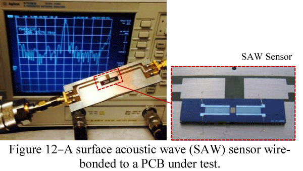
Figure 12:
FPCBs have also been used for MEMS packaging [59-61]. The flexibility of flexible PCBs is beneficial in terms of reducing the size and weight of the final device because the PCB can bend or take the shape of the final structure. However, the cost of its prototyping is much higher than the conventional PCBs. Figure 13 demonstrates MEMS sensors along with electrical modules packaged on a FPCB to be mounted on a structure.
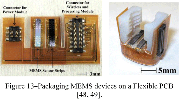
Figure 13:
Usually bonding MEMS device on PCB is used for sensors which do not need base excitation to function. However, due to very small deflections (≤1mm) of MEMS resonators, conventional solid PCBs with ~1.5mm thickness can be used for primary testing purposes. Figure 14 demonstrates a PCB designed with a hole in the middle to provide space for the oscillation of the proof mass of an energy harvester. Wire-bonding and soldering are used to make electrical connections.
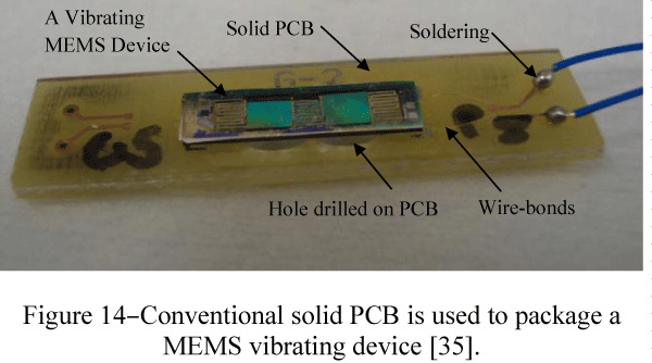
Figure 14:
Packaging with a mechanical support
In some cases especially for resonators, the MEMS device(s) and PCBs have to be a structure [62-66]. The structure could be as simple as Figure 15 where two polymer sheets are cut and glued such that there is enough space for the cantilever's proof mass to vibrate. However due to mass production and reliability issues, a more robust method must be chosen. In this section, 3D printing is proposed as an alternative.
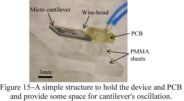
Figure 15:
Lately, MEMS inertial sensor
s are in transition from fully hermetic ceramic to plastic packaging that helps meet their price margins [1]. 3D printing is a cheap and quick manufacturing technique
to build such tiny structures and customize them for special shapes and designs. In addition, researchers have recently developed, and are still working on, developing biocompatible materials to be used for 3D printing machineries [67-71]. These materials could also be exploited to make packaging structures for covering energy harvesters from its environment for use with biological systems. 3D printing could also be used for the prototyping stage to keep the costs down. Figure 16 demonstrates customizing a structure design to mechanically support both a MEMS device and a tiny PCB. Wire-bonding and soldering was used to make electrical connections. The 3D printed part was designed such that it could be clamped to the shaker table (Figure 17). To make the 3D printing parts, an Eden 350V from Object was used with high resolution layers of 16μm in Z axis, accuracy of 0.1-0.3 mm and with glossy quality.
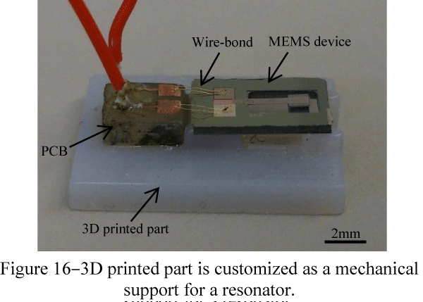
Figure 16:
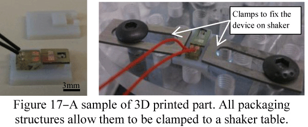
Figure 17:
3D printing could also be considered for sealed box packages to completely protect the device from its environment (Figure 18). Various dispensing adhesives or laser sealing which are used to seal plastic packages [1] could be exploited to seal the lid to the bottom of a 3D printed structure. MEMS ink-jet chip packaging, capping process and thermoplastic injection molding are some of the other methods to build a structure to protect the chip from its environment. However, none of them is as fast, cheap and customizable as the 3D printing process.
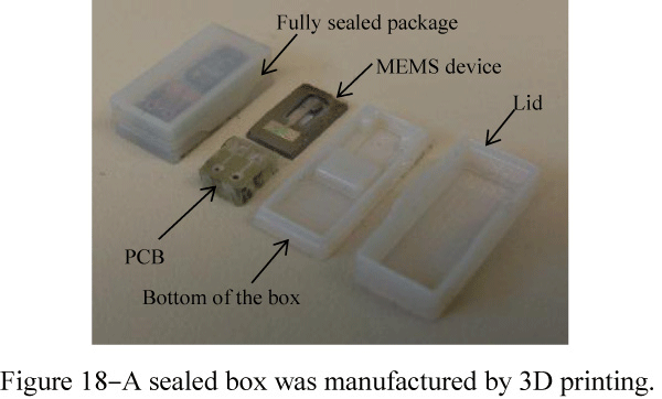
Figure 18:
Package for Under Vacuum Pretest
Testing under vacuum would decrease the air damping effect and consequently increase the quality factor of a resonator. In the case of an energy harvester, a device under vacuum would have higher vibration amplitude which in turn causes higher output energy for the same excitation amplitude. Researchers would always prefer to package their devices under vacuum to improve the output results [72-75]. Various techniques have been developed for chip-level and wafer-level vacuum packaging of MEMS devices [76-82]. However, before pursuing a vacuum packaging process, one would like to test and characterize the fabricated MEMS device under vacuum. Considering the low yield of any packaging technique in general, it would be beneficial to test a device under vacuum before it is fully packaged.
A small chamber has been designed and built to ease the primarily testing and characterization steps. This low cost chamber is shown in Figure 19. The main body is made by 3D printing. The cap is a glass slide to allow a laser to shine on the MEMS device and make vertical displacement measurements. Two thin wires are vacuum sealed and provide electrical connections across the chamber. A connector to the vacuum pump and a spring clamp to hold the MEMS devices inside the chamber are the other components of this design. Using this chamber, any MEMS devices could be tested under vacuum to ensure its functionality before any further processing.

Figure 19:
Conclusion
A number of 3D micro-assembly techniques have been demonstrated in this article to electrically and mechanically package MEMS devices. In terms of electrical interconnections, wire-bonding, tape automated bonding, adhesive-based bonding and flip-chipping were examined and a number of sample prototypes were presented for each case which were developed or adapted in our lab. Additionally, an improvised application of flexible and conventional solid PCBs was demonstrated to bond to MEMS devices and allow electrical characterization. In addition, a low cost technique was developed to use a manual dispenser and precisely dispense adhesive dots for MEMS packaging applications. Besides, 3D printing was exploited to build customizable mechanical packages for MEMS devices. This technique is expandable for bio MEMS applications as well due to the capability of 3D printing technology to build structures with bio-compatible materials. Finally, a small vacuum chamber was designed to examine mechanical responses of micro-resonators under vacuum before finalizing their electrical and mechanical packaging. The packaging methods in this article were practically shown on prototype MEMS devices to provide a platform to deal with some of the main 3D packaging challenges; however by slightly tweaking them, many can be used for mass production purposes as well.
Acknowledgement
Authors would like to thank CMC Microsystems, NSERC (Natural Sciences and Engineering Research Council of Canada) and AITF (Alberta Innovates-Technology Futures) for providing micro fabrication funding.
References
- Gilleo K. MEMS/MOEM Packaging: Concepts, Designs, Materials and Processes: McGraw-Hill Professional Publishing. 2005.
- John H, Lau CL, Premachandran CS, Yu Aibin. Bio-MEMS Packaging: McGraw-Hill Professional. 2010; 2010.
- Wong CP, Moon KS, Li Y. Nano-Bio- Electronic, Photonic and MEMS Packaging: Springer. 2009.
- Tekin T. Review of Packaging of Optoelectronic, Photonic, and MEMS Components. Ieee J Sel Top Quant. 2011; 17: 704-719.
- Lucyszyn S. Review of radio frequency micro electromechanical systems technology. Iee P-Sci Meas Tech. 2004; 151: 93-103.
- Madou MJ. Fundamentals of Micro fabrication: The Science of Miniaturization, Second Edition: Taylor & Francis. 2002.
- Senturia SD. Microsystem Design: Springer. 2000.
- Shoji S, Kikuchi H, Torigoe H. Low-temperature anodic bonding using lithium aluminosilicate-beta-quartz glass ceramic. Sensor Actuat a-Phys. 1998; 64: 95-100.
- Maluf N, Williams K. Introduction to Micro electromechanical Systems Engineering: Artech House. 2004.
- Ramesham R, Ghaffarian R. Challenges in interconnection and packaging of micro electromechanical systems (MEMS). P Electr C. 2000: 666-675.
- Morrissey A, Kelly G, Alderman J. Selection of materials for reduced stress packaging of a micro system. Sensor Actuat a-Phys. 1999; 74: 178-181.
- Butler JT, Bright VM, Comtois JH. Multichip module packaging of micro electromechanical systems. Sensor Actuat a-Phys. 1998; 70: 15-22.
- Bustillo J, Fedder G, Nguyen CC, Howe R. Process technology for the modular integration of CMOS and polysilicon microstructures. Microsystem Technologies. 1994; 1: 30-41.
- Tilmans HAC, De Raedt W, Beyne E. MEMS for wireless communications: 'from RF-MEMS components to RF-MEMS-SiP'. J Micromech Microeng. 2003; 13: S139-S63.
- Viswanadham P. Essentials of Electronic Packaging: A Multidisciplinary Approach: American Society of Mechanical Engineers. 2011.
- Ganesh VP, Lee C. Overview and emerging challenges in mechanical dicing of silicon wafers. El Packag Tech Conf. 2006; 15-21.
- Enikov ET, Nelson BJ. Three-dimensional microfabrication for a multi-degree-of-freedom capacitive force sensor using fibre-chip coupling. J Micromech Microeng. 2000; 10: 492-497.
- Gradin H, Braun S, Sterner M, Stemme G, van der Wijngaart W. Selective electrochemical release etching of eutectically bonded microstructures. Solid-State Sensors, tuators and Microsystems Conference, 2009 TRANSDUCERS 2009 International. 2009; 743-746.
- Tseng SH, Xiao FY, Juang YZ, Chiu CF, Cheng MC. Solutions for dicing released CMOS-MEMS multi-project wafer. Design, test, integration and packaging of EMS; DTIP 2004. 2004: 55-60.
- Oliver AD, Wallner TA, Tandon R, Nieman K, Bergstrom PL. Diamond scribing and breaking of silicon for MEMS die separation. J Micromech Microeng. 2008; 18.
- Misra A, Fininie I. On the scribing and subsequent fracturing of silicon semiconductor wafers. J Mater Sci. 1979; 14: 2567-2574.
- Ogorodnikov AI, Ogorodnikova OM, Tikhonov IN. Simulation of defect zones in scribed silicon wafers. Iop Conf Ser-Mat Sci. 2010; 15.
- Heriban D, Agnus J, Petrini V, Gauthier M. A mechanical de-tethering technique for silicon MEMS etched with a DRIE process. J Micromech Microeng. 2009; 19.
- Xie J, Hao Y, Shen Q, Chang H, Yuan W. A dicing-free SOI process for MEMS devices based on the lag effect. J Micromech Microeng. 2013; 23.
- Sari I, Zeimpekis L, Kraft M. A dicing free SOI process for MEMS devices. Micro electron Eng. 2012; 95: 121- 129.
- Qu HW, Xie HK. Process development for CMOS-MEMS sensors with robust electrically isolated bulk silicon microstructures. J Micro electro mech S. 2007; 16: 1152-1161.
- Pau S, Taylor JA, Pai CS. Nonorthogonal wafer dicing for waveguide, microelectromechanical systems, and nanotechnology applications. J Vac Sci Technol B. 2004; 22: L15-L6.
- Porter DA, Berfield TA. Die separation and rupture strength for deep reactive ion etched silicon wafers. J Micromech Microeng. 2013; 23.
- Sari I, Zeimpekis I, Kraft M. A Full Wafer Dicing Free Dry Release Process for MEMS Devices. Procedia Engineer. 2010; 5: 850-853.
- Rezaei M, Lueke J, Sameoto D, Raboud D, Moussa W. A New Approach to Cleave MEMS Devices from Silicon Substrates. Journal of Mechanics Engineering and Automation. 2013; 3: 731-738.
- Ginsberg GL, Schnorr DP. Multichip modules and related technologies: MCM, TAB, and COB design: McGraw-Hill; 1994.
- Blackwell GR. The Electronic Packaging Handbook: Taylor & Francis. 1999.
- Hsu TR. Mems Packaging: Institution of Engineering and Technology; 2004.
- Benfield D, Lueke J, Moussa W. MEMS Packaging Using Flexible Printed Circuit Boards. CMC Microsystems Application Note, CMC-00200-01607: CMC Microsystems. 2011; 12.
- Lueke JS. A MEMS-based Fixed-Fixed Folded Spring Piezoelectric Energy Harvester [PhD Dissertation]: University of Alberta; 2014.
- Cao YH, Ning WG, Luo L. Wafer-Level Package With Simultaneous TSV Connection and Cavity Hermetic Sealing by Solder Bonding for MEMS Device. Ieee T Electron Pack. 2009; 32:125-232.
- Dixit P, Salonen J, Pohjonen H, Monnoyer P. The application of dry photoresists in fabricating cost-effective tapered through-silicon vias and redistribution lines in a single step. J Micromech Microeng. 2011; 21.
- Jackson N, Muthuswamy J. Flexible Chip Scale Package and Interconnect for Implantable MEMS Movable Microelectrodes for the Brain. See comment in PubMed Commons below J Microelectromech Syst. 2009; 18: 396-404.
- Joung YH, Allen MG. A micromachined chip-to-board interconnect system using electroplating bonding technology. Ieee T Adv Packaging. 2008; 31: 357-366.
- Jozwiak J, Southwick RG, Johnson VN, Knowlton WB, Moll AJ. Integrating through-wafer interconnects with active devices and circuits. Ieee T Adv Packaging. 2008; 31: 4-13.
- Tian J, Sosin S, Lannacci J, Gaddi R, Bartek M. RF-MEMS wafer-level packaging using through-wafer interconnect. Sensor Actuat a-Phys. 2008; 142: 442-451.
- Ji F, Leppadvuori E, Luusua I, Hentfinen K, Eranen S, Hietanen H, et al. Fabrication of silicon based through-wafer interconnects for advanced chip scale packaging. Sensor Actuat a-Phys. 2008; 142: 405-412.
- Chow EM, Chandrasekaran V, Partridge A, Nishida T, Sheplak M, Quate CF, et al. Process compatible polysilicon-based electrical through-wafer interconnects in silicon substrates. J Microelectromech S. 2002; 11: 631-640.
- Ham YH, Kim DP, Park KS, Jeong YS, Yun HJ, Baek KH, et al. Dual etch processes of via and metal paste filling for through silicon via process. Thin Solid Films. 2011; 519: 6727-6731.
- Lee SWR, Hon R, Zhang SXD, Wong CK. 3D stacked flip chip packaging with through silicon vias and copper plating or conductive adhesive filling. Elec Comp C. 2005:795-801.
- Kikuchi H, Yamada Y, Ali AM, Liang J, Fukushima T, Tanaka T, et al. Tungsten through-silicon via technology for three-dimensional LSIs. Jpn J Appl Phys. 2008; 47: 2801-2806.
- Fischer AC, Grange M, Roxhed N, Weerasekera R, Pamunuwa D, Stemme G, et al. Wire-bonded through-silicon vias with low capacitive substrate coupling. J Micromech Microeng. 2011; 21.
- Benfield D, Lou E, Moussa WA. A packaging solution utilizing adhesive-filled TSVs and flip-chip methods. J Micromech Microeng. 2012; 22.
- Benfield DC. A Study of Six-Axis MEMS Sensors for Load Detection in Biomedical Applications [PhD Dissertation]: University of Alberta; 2012.
- Gharib HMH. An investigation of using n-Si piezoresistive behavior to develop a three-dimensional stress sensing rosette [PhD Dissertation]: University of Alberta. 2013.
- Esashi M. Wafer level packaging of MEMS. J Micromech Microeng. 2008; 18.
- Gharib HH, Moussa WA. Testing of a single-polarity piezoresistive three-dimensional stress-sensing chip. J Micromech Microeng. 2013; 23.
- Rezaei M, Lueke J, Raboud D, Moussa W. Challenges in fabrication and testing of piezoelectric MEMS with a particular focus on energy harvesters. Microsyst Technol. 2013; 19: 1195-1219.
- Campanella H, Nouet P, De Paco P, Uranga A, Barniol N, Esteve J. Automated on-wafer characterization in micro-machined resonators: towards an integrated test vehicle for bulk acoustic wave resonators (FBAR). Ieee Int C Microelec. 2007:157-161.
- Oh H, Lee K, Eun K, Choa SH, Yang SS. Development of a high-sensitivity strain measurement system based on a SH SAW sensor. J Micromech Microeng. 2012; 22.
- Johansson L, Enlund J, Johansson S, Katardjiev I, Yantchev V. Surface acoustic wave induced particle manipulation in a PDMS channel--principle concepts for continuous flow applications. See comment in PubMed Commons below Biomed Microdevices. 2012; 14: 279-289.
- Nicolay P, Elmazria O, Sarry F, Aubert T, Bouvot L, Hehn M. New Measurement Method to Characterize Piezoelectric SAW Substrates at Very High Temperature. Ultrason. 2008: 1877-1880.
- Yi-Tian L, Hsu-Chao H, Mei-Ching C, Tai-Hsuan L, Pei-Hsin K, Chia-Min Y, et al. Polymer-coated surface acoustic wave sensor array for low concentration NH3 detection. Nano/Micro Engineered and Molecular Systems (NEMS). IEEE International Conference on 2011; 333-337.
- Siegel AC, Phillips ST, Dickey MD, Lu NS, Suo ZG, Whitesides GM. Foldable Printed Circuit Boards on Paper Substrates. Adv Funct Mater. 2010; 20: 28-35.
- Ramadoss R, Lee S, Lee YC, Bright VM, Gupta KC. Fabrication, assembly, and testing of RF MEMS capacitive switches using flexible printed circuit technology. Ieee T Adv Packaging. 2003; 26: 248-254.
- Lee S, Ramadoss R, Buck M, Bright VM, Gupta KC, Lee YC. Reliability testing of flexible printed circuit-based RF MEMS capacitive switches. Microelectronics Reliability. 2004; 44: 245-250.
- Wang PH, Tanaka K, Sugiyama S, Dai XH, Zhao XL, Liu JQ. A micro electromagnetic low level vibration energy harvester based on MEMS technology. Microsyst Technol. 2009; 15: 941-951.
- Elfrink R, Kamel TM, Goedbloed M, Matova S, Hohlfeld D, van Andel Y, et al. Vibration energy harvesting with aluminum nitride-based piezoelectric devices. J Micromech Microeng. 2009; 19.
- Miao P, Mitcheson PD, Holmes AS, Yeatman EM, Green TC, Stark BH. Mems inertial power generators for biomedical applications. Microsyst Technol. 2006; 12: 1079-1083.
- Aktakka EE, Peterson RL, Najafi K. A Self-Supplied Inertial Piezoelectric Energy Harvester with Power-Management IC. In: IEEE, editor. 2011 IEEE International Solid-State Circuits Conference. Beijing, China. 2011; 120-121.
- Liu JQ, Fang HB, Xu ZY, Mao XH, Shen XC, Chen D, et al. A MEMS-based piezoelectric power generator array for vibration energy harvesting. Microelectron J. 2008; 39: 802-506.
- Khalyfa A, Vogt S, Weisser J, Grimm G, Rechtenbach A, Meyer W, et al. Development of a new calcium phosphate powder-binder system for the 3D printing of patient specific implants. J Mater Sci Mater Med. 2007; 18: 909-916.
- Warnke PH, Seitz H, Warnke F, Becker ST, Sivananthan S, Sherry E, et al. Ceramic scaffolds produced by computer-assisted 3D printing and sintering: characterization and biocompatibility investigations. J Biomed Mater Res B Appl Biomater. 2010; 93: 212-217.
- Peltola SM, Melchels FP, Grijpma DW, Kellomäki M. A review of rapid prototyping techniques for tissue engineering purposes. Ann Med. 2008; 40: 268-280.
- Seitz H, Rieder W, Irsen S, Leukers B, Tille C. Three-dimensional printing of porous ceramic scaffolds for bone tissue engineering. J Biomed Mater Res B Appl Biomater. 2005; 74: 782-788.
- Pfister A, Landers R, Laib A, Hubner U, Schmelzeisen R, Mulhaupt R. Biofunctional rapid prototyping for tissue-engineering applications: 3D bioplotting versus 3D printing. J Polym Sci Pol Chem. 2004; 42: 624-638.
- Yang B, Lee C, Kotlanka RK, Xie J, Lim SP. A MEMS rotary comb mechanism for harvesting the kinetic energy of planar vibrations. J Micromech Microeng. 2010; 20.
- Elfrink R, Renaud M, Kamel TM, de Nooijer C, Jambunathan M, Goedbloed M, et al. Vacuum-packaged piezoelectric vibration energy harvesters: damping contributions and autonomy for a wireless sensor system. J Micromech Microeng. 2010; 20.
- Williams CB, Shearwood C, Harradine MA, Mellor PH, Birch TS, Yates RB. Development of an electromagnetic micro-generator. Circuits, Devices and Systems, IEE Proceedings -. 2001; 148: 337-342.
- Lee C, Lima YM, Yang B, Kotlanka RK, Heng CH, He JH, et al. Theoretical comparison of the energy harvesting capability among various electrostatic mechanisms from structure aspect. Sensor Actuat a-Phys. 2009; 156: 208-216.
- Gooch R, Schimert T. Low-Cost Wafer-Level Vacuum Packaging for MEMS. MRS Bulletin. 2003; 28: 55-59.
- Topalli ES, Topalli K, Alper SE, Serin T, Akin T. Pirani Vacuum Gauges Using Silicon-on-Glass and Dissolved-Wafer Processes for the Characterization of MEMS Vacuum Packaging. Ieee Sens J. 2009; 9: 263-270.
- Chae J, Giachino JM, Najafi K. Fabrication and characterization of a wafer-level MEMS vacuum package with vertical feed throughs. J Microelectromech S. 2008; 17: 193-200.
- Sparks DR, Massoud-Ansari S, Najafi N. Chip-level vacuum packaging of micro machines using Nano Getters. Ieee T Adv Packaging. 2003; 26: 277-282.
- Cheng YT, Hsu WT, Najafi K, Nguyen CTC, Lin LW. Vacuum packaging technology using localized aluminum/silicon-to-glass bonding. J Micro electromech S. 2002; 11: 556-565.
- Lee B, Seok S, Chun K. A study on wafer level vacuum packaging for MEMS devices. J Micromech Microeng. 2003; 13: 663-669.
- Welch WC, Najafi K. Gold-indium transient liquid phase (TLP) wafer bonding for MEMS vacuum packaging. Mems 2008: 21st Ieee International Conference on Micro Electro Mechanical Systems, Technical Digest. 2008: 806-809.