Editorial
Austin J Nanomed Nanotechnol. 2014;2(6): 1033.
Graphene Based Nano Electromechanical Interconnects to Enable Ultrafast Electronics
Mustafa Yavuz1*, Mehrdad Irannejad1, Kamil Alici2, Eihab Abdel Rahman1, Andrew Brzezinski1 and Bo Cui1
1Waterloo Institute for Nanotechnology, University of Waterloo, Canada
2TUBITAK Marmara Research Center, Turkey
*Corresponding author: Mustafa Yavuz, Waterloo Institute For Nanotechnology, University of Waterloo, Ontario Canada
Received: August 30, 2014; Accepted: September 08, 2014; Published: September 10, 2014
Editorial
Integration of nano electromechanical systems (NEMS) to current complementary metal oxide semiconductor (CMOS) chips significantly reduces the contact resistance of electronic devices and enables high speed electronics. However, NEMS devices suffer from packaging problems and their performance parameters in durability and reliability are low. Utilizing graphene in NEMS provides exceptional structural, mechanical, thermal and electrical properties for the interconnections and thereby constitutes a promising solution for high performance packaging and electronic applications.
Graphene is a collection of sp2 bonded carbon atoms arranged in a two-dimensional honeycomb shaped lattice. It is optically transparent with highly accessible surface area and has an exceptionally high electrical conductivity. Its unique electrical properties such as ballistic electron transport are attributed to its planar conjugate bonds. Theoretically, graphene has the highest electron mobility (200000 cm2/Vs), highest thermal conductivity (4000 W/mK), largest elastic modulus (10TPa), highest hardness (217 kgf/mm), largest yielding strength (6.4TPa) and largest tensile strength (130GPa that is three orders of magnitude larger than A36 steel's) among all known materials. We anticipate that hybridization of graphene with compatible materials (MoS2, BN, and WS2) is going to create unique opportunities at nano scale. Optimization of such graphene based interconnections for specific devices such as sensors and transparent electrodes is very interesting for the N/MEMS community. The proposed interconnections are micro-bonded and encapsulated with light weighted and cost effective polymers providing high thermal resistance [1-8].
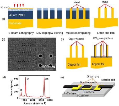
The fabrication of copper nano wire arrays, growth of graphene on the top of copper nano wire arrays, transfer of graphene coated nano wire arrays to graphene coated Silicon on SiO2 substrate, fabrication of contact pads and polymer encapsulation are the main steps of the device fabrication. These steps are briefly described in Figure 1. E-beam lithography and electroplating are followed by atomic force microscopy, scanning tunneling microscopy, four probe lock measurements at cryogenic temperatures for the copper nano wire array fabrication and characterization. Chemical vapor deposition of carbon forms monolayer graphene on nano wire arrays on which polymethyl methacrylate is spin coated and bulky parts of the copper foils are etched away by using an aqueous solution of Fe(NO3)3. Films are physically transferred to commercially available graphene coated SiO2 on Si substrates on which metal electrodes are formed with ultraviolet lithography. The PMMA is then dissolved and removed by using conventional solutions. A few step special process recipes finalizes contact electrode and top gate fabrication as sketched in Figure 1 (e). Mechanical and electrical properties of the graphene integrated parts are tested by multiple techniques including AFM, SEM, transmission electron microscope (TEM), Raman Spectroscopy (RS) with various wavelength laser sources, nano-indentation and four-probe lock-in technique at cryogenic temperatures. At the graphene interfaces utilization MoS2, BN or WS2 buffer layers is of significant importance to achieve the desired performance parameters [9-12].
Figure 1: (a) Schematic that demonstrates the fabrication steps. (b) SEM graph of fabricated nanowires. (c) Schematic diagram of graphene film deposition around copper nanorods/nanowires (d) Raman spectrum data of multilayer graphene films (e) Schematic diagram of graphene/metal nanostructure fabrication through lithography method and metal deposition as connection pad.
Interconnections are one of the most significant components of every electronic device. Recently, miniaturization of electronic devices required extensive utilization nanotechnology. In the present paper, we have proposed and demonstrated an interconnect that utilizes graphene hybridized NEMS. It provides durable and reliable packaging properties and is suitable for high speed electronics applications.
References
- Miao F, Wijeratne S, Zhang Y, Coskun UC, Bao W, Lau CN. Phase-coherent transport in graphene quantum billiards. Science. 2007; 317: 1530-1533.
- Castro Neto AH, Guinea F, Peres NMR, Novoselov KS, Geim AK. The electronic properties of graphene. Reviews of Modern Physics. 2009; 81: 109-162.
- Nilsson J, Neto AH, Guinea F, Peres NM. Electronic properties of graphene multilayers. Phys Rev Lett. 2006; 97: 266801.
- Chamanara N, Sounas D, Szkopek T, Caloz C. Optically Transparent and Flexible Graphene Reciprocal and Nonreciprocal Microwave Planar Components. Microwave and Wireless Components Letters, IEEE. 2012; 22: 360-362.
- Ranjbartoreh AR, Wang B, Shen X, Wang G. Advanced mechanical properties of graphene paper. Journal of Applied Physics. 2011; 109.
- Carpenter C, Christmann AM, Hu L, Fampiou I, Muniz AR, Ramasubramaniam A, et al. Elastic properties of graphene nanomeshes. Applied Physics Letters. 2014; 104.
- Ibrahim KM, Irannejad M, Ramadhan A, Alayak W, Sandeson J, Cui B, et al. Ultrafast light interaction with Graphene oxide aqueous solution. In: Publication I edn. 14th International Conference on Nanotechnology, Toronto, Canada. 2012.
- HosseinMousavi S, Iskandar Kholmanov, Kamil B Alici, David Purtseladze, NihalArju, Kaya Tatar, et al. Ruoff, and Gennady Shvets "Inductive Tuning of Fano-Resonant Metasurfaces Using Plasmonic Response of Graphene in the Mid-Infrared". Nano Letters. 2013; 13: 1111-1117.
- Irannejad M, Zhang J, Yavuz M, Cui B. Numerical Study of Optical Behavior of Nano-Hole Array with Non-Vertical Sidewall Profile. Plasmonics. 2014; 9: 537-544.
- Li X, Zhu Y, Cai W, Borysiak M, Han B, Chen D, et al. Transfer of large-area graphene films for high-performance transparent conductive electrodes. Nano Lett. 2009; 9: 4359-4363.
- Ferrari AC. Raman spectroscopy of graphene and graphite: Disorder, electron-phonon coupling, doping and nonadiabatic effects. Solid State Communications. 2007; 143: 47-57.
- Gu Z, Ye H, Gracias D, Gracias D. The bonding of nanowire assemblies using adhesive and solder. 2005; 57: 60-64.
